All posts by Xiaomin Shen

Introducing the Project Argus Datacenter-ready Secure Control Module design specification

Post Syndicated from Xiaomin Shen original http://blog.cloudflare.com/introducing-the-project-argus-datacenter-ready-secure-control-module-design-specification/

Introducing the Project Argus Datacenter-ready Secure Control Module design specification

Introducing the Project Argus Datacenter-ready Secure Control Module design specification

Historically, data center servers have used motherboards that included all key components on a single circuit board. The DC-SCM (Datacenter-ready Secure Control Module) decouples server management and security functions from a traditional server motherboard, enabling development of server management and security solutions independent of server architecture. It also provides opportunities for reducing server printed circuit board (PCB) material cost, and allows unified firmware images to be developed.

Today, Cloudflare is announcing that it has partnered with Lenovo to design a DC-SCM for our next-generation servers. The design specification has been published to the OCP (Open Compute Project) contribution database under the name Project Argus.

A brief introduction to baseboard management controllers

A baseboard management controller (BMC) is a specialized processor that can be found in virtually every server product. It allows remote access to the server through a network connection, and provides a rich set of server management features. Some of the commonly used BMC features include server power management, device discovery, sensor monitoring, remote firmware update, system event logging, and error reporting.

In a typical server design, the BMC resides on the server motherboard, along with other key components such as the processor, memory, CPLD and so on. This was the norm for generations of server products, but that has changed in recent years as motherboards are increasingly optimized for high-speed signal bandwidth, and servers need to support specialized security requirements. This has made it necessary to decouple the BMC and its related components from the server motherboard, and move them to a smaller common form factor module known as the Datacenter Secure Control Module (DC-SCM).

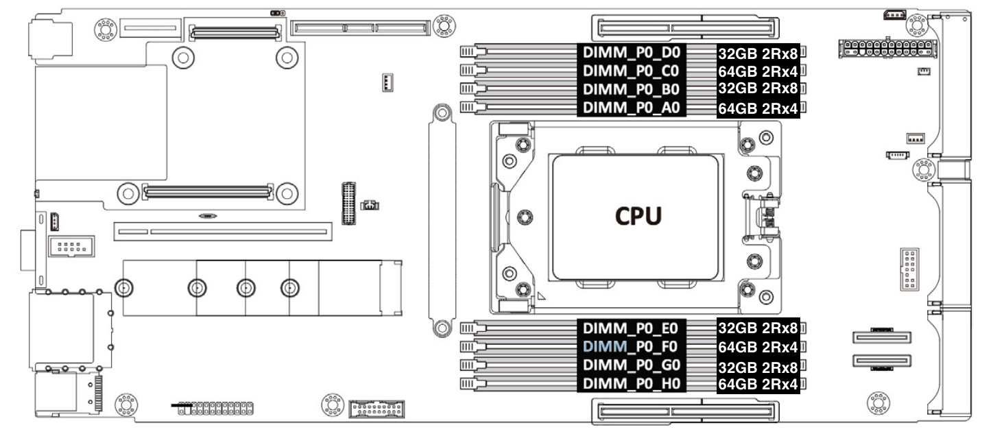
Figure 1 is a picture of a motherboard used on Cloudflare’s previous generation of edge servers. The BMC and its related circuit components are placed on the same printed circuit board as the host CPU.

Introducing the Project Argus Datacenter-ready Secure Control Module design specification
Figure 1: Previous Generation Server Motherboard

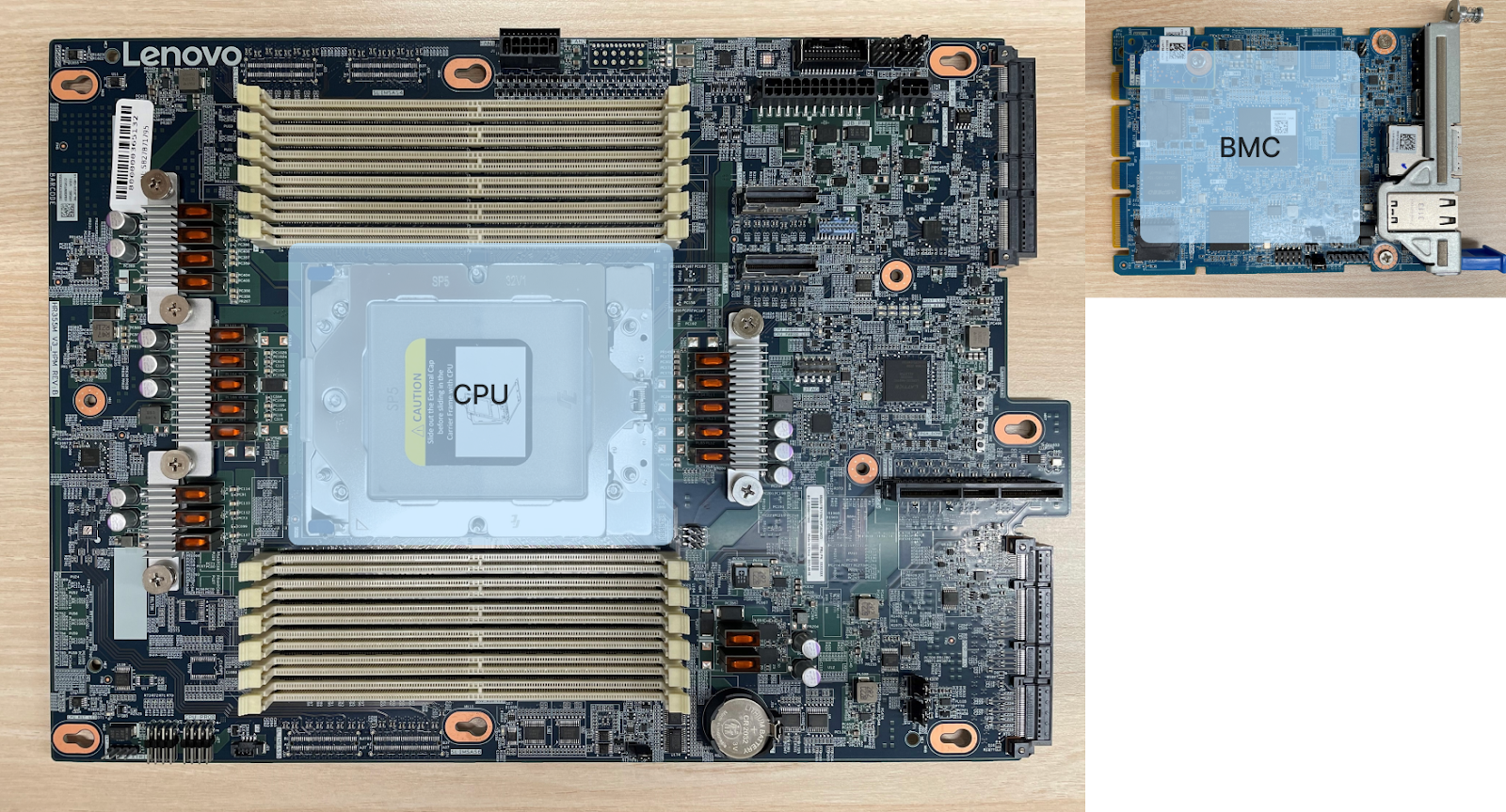
For Cloudflare’s next generation of edge servers, we are partnering with Lenovo to create a DC-SCM based design. On the left-hand side of Figure 2 is the printed circuit board assembly (PCBA) for the Host Processor Module (HPM). It hosts the CPU, the memory slots, and other components required for the operation and features of the server design. But the BMC and its related circuits have been relocated to a separate PCBA, which is the DC-SCM.

Introducing the Project Argus Datacenter-ready Secure Control Module design specification
Figure 2: Next Generation HPM and DC-SCM

Benefits of DC-SCM based server design

PCB cost reduction

As of today, DDR5 memory runs at 6400MT/s (mega transfers per second). In the future DDR5 speed may even increase to 7200MT/s or 8800MT/s. Meanwhile, PCIe Gen5 is running at 32 GT/s (giga transfers per second), doubling the speed rate of PCIe Gen4. Both DDR5 and PCIE Gen5 are key interfaces for the processors used on our next-generation servers.

The increasing rates of high-speed IO signals and memory buses are pushing the next generation of server motherboard designs to transition from low-loss to ultra-low loss dielectric printed circuit board (PCB) materials, and higher layer counts in the PCB. At the same time, the speed of BMC and its related circuitry are not progressing so quickly. For example, the physical layer interface of ASPEED AST2600 BMC is only at PCIe Gen2 (5 GT/s).

Ultra-low loss dielectric PCB material and higher PCB layer count are both driving factors for higher PCB cost. Another driving factor of PCB cost is the size of the PCB. In a traditional server motherboard design, the size of the server motherboard is larger, since the BMC and its related circuits are placed on the same PCB as the host CPU.

By decoupling the BMC and its related circuitry from the host processor module (HPM), we can reduce the size of the relatively more expensive PCB for the HPM. BMC and its related circuitry can be placed on relatively cheaper PCB, with reduced layer count and lossier PCB dielectric materials. For example, in the design of Cloudflare’s next generation of servers, the server motherboard PCB needs to be 14 or more layers, whereas the BMC and its related components can be easily routed with 8 or 10 layers of PCB. In addition, the dielectric material used on DC-SCM PCB is low-loss dielectric — another cost saver compared to ultra-low loss dielectric materials used on HPM PCB.

Modularized design enables flexibility

DC-SCM modularizes server management and security components into a common add-in card form factor, enabling developers to remove customer specific solutions from the more complex components, such as motherboards, to the DC-SCM. This provides flexibility for developers to offer multiple customer-specific solutions, without the need to redesign multiple motherboards for each solution.

Developers are able to reuse the DC-SCM from a previous generation of server design, if the management and security requirements remain the same. This reduces the overall cost of upgrading to a new generation of servers, and has the potential to reduce e-waste when a server is decommissioned.

Likewise, management and security solution upgrades within a server generation can be carried out separately by modifying or replacing the DC-SCM. The more complex components on the HPM do not need to be redesigned. From a data center perspective, it speeds up the upgrade of management and security hardware across multiple server platforms.

Unified interoperable OpenBMC firmware development

Data center secure control interface (DC-SCI) is a standardized hardware interface between DC-SCM and the Host Processor Module (HPM). It provides a basis for electrical interoperability between different DC-SCM and host processor module (HPM) designs.

This interoperability makes it possible to have a unified firmware image across multiple DC-SCM designs, concentrating development resources on a single firmware rather than an array of them. The publicly-accessible OpenBMC repository provides a perfect platform for firmware developers of different companies to collaborate and develop such unified OpenBMC images. Instead of maintaining a separate BMC firmware image for each platform, we now use a single image that can be applied across multiple server platforms. The device tree specific to each respective server is automatically loaded based on device product information.

Using a unified OpenBMC image significantly simplifies the process of releasing BMC firmware to multiple server platforms. Firmware updates and changes are propagated to all supported platforms in a single firmware release.

Project Argus

The DC-SCM specifications have been driven by the Open Compute Project (OCP) Foundation hardware management workstream, as a way to standardize server management, security, and control features.

Cloudflare has partnered with Lenovo on what we call Project Augus, Cloudflare’s first DC-SCM implementation that fully adheres to the DC-SCM 2.0 specification. In the DC-SCM 2.0 specifications, a few design items are left open for implementers to decide on the most suitable architectural choices. With the goal of improving interoperability of Cloudflare DC-SCM designs across server vendors and server designs, Project Argus includes documentation on implementation details and design decisions on form factor, mechanical locking mechanism, faceplate design, DC-SCI pin out, BMC chip, BMC pinout, Hardware Root of Trust (HWRoT), HWRoT pinout, and minimum bootable device tree.

Introducing the Project Argus Datacenter-ready Secure Control Module design specification
Figure 3: Project Argus DC-SCM 2.0

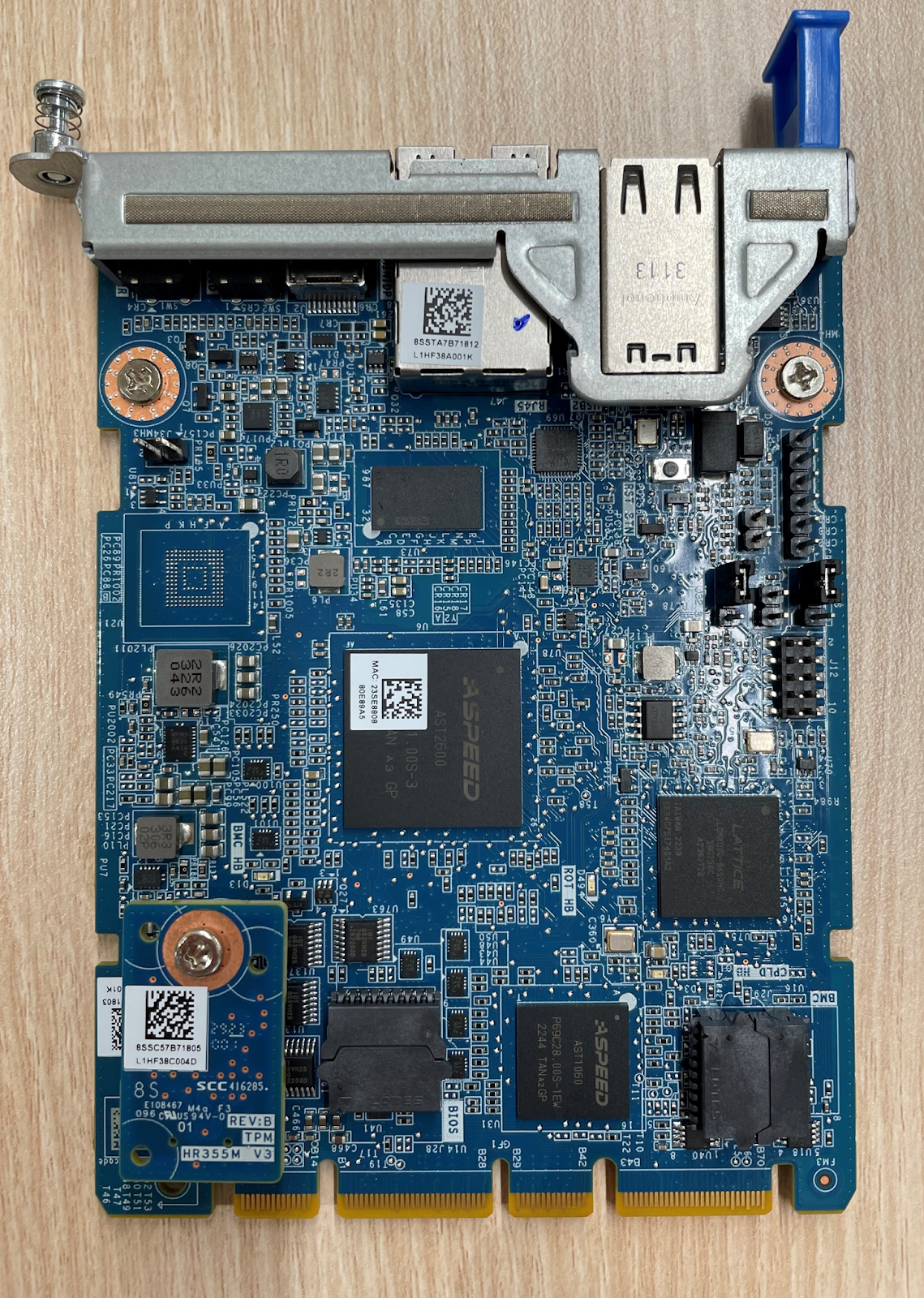
At the heart of the Project Argus DC-SCM is the ASPEED AST2600 BMC System on Chip (SoC), which when loaded with a compatible OpenBMC firmware, provides a rich set of common features necessary for remote server management. ASPEED AST1060 is used on Project Argus DC-SCM as the HWRoT solution, providing secure firmware authentication, firmware recovery, and firmware update capability. Project Argus DC-SCM 2.0 uses Lattice MachXO3D CPLD with secure boot and dual boot ability as the DC-SCM CPLD to support a variety of IO interfaces including LTPI, SGPIO, UART and GPIOs.

The mechanical form factor of Project Argus DC-SCM 2.0 is the horizontal External Form Factor (EFF).

Cloudflare and Lenovo have contributed Project Argus Design Specification and reference design files to the OCP contribution database. Below is a detailed list of our contribution:

  • SPI, I2C/I3C, UART, LTPI/SGPIO block diagrams
  • DC-SCM PCB stackup
  • DC-SCM Board placements (TOP and BOTTOM layers)
  • DC-SCM schematic PDF file
  • DC-SCI pin definition PDF file
  • Power sequence PDF file
  • DC-SCM bill of materials Excel spreadsheet
  • Minimum bootable device tree requirements
  • Mechanical Drawings PDF files, including card assembly drawing and interlock rail drawing

The security foundation for our Gen 12 hardware

Cloudflare has been innovating around server design for many years, delivering increased performance per watt and reduced carbon footprints. We are excited to integrate Project Argus DC-SCM 2.0 into our next-generation, Cloudflare Gen 12 servers. Stay tuned for more exciting updates on Cloudflare Gen 12 hardware design!

DDR4 memory organization and how it affects memory bandwidth

Post Syndicated from Xiaomin Shen original https://blog.cloudflare.com/ddr4-memory-organization-and-how-it-affects-memory-bandwidth/

DDR4 memory organization and how it affects memory bandwidth

DDR4 memory organization and how it affects memory bandwidth

When shopping for DDR4 memory modules, we typically look at the memory density and memory speed. For example a 32GB DDR4-2666 memory module has 32GB of memory density, and the data rate transfer speed is 2666 mega transfers per second (MT/s).

If we take a closer look at the selection of DDR4 memories, we will then notice that there are several other parameters to choose from. One of them is rank x organization, for example 1Rx8, 2Rx4, 2Rx8 and so on. What are these and does memory module rank and organization have an effect on DDR4 module performance?

In this blog, we will study the concepts of memory rank and organization, and how memory rank and organization affect the memory bandwidth performance by reviewing some benchmarking test results.

Memory rank

Memory rank is a term that is used to describe how many sets of DRAM chips, or devices, exist on a memory module. A set of DDR4 DRAM chips is always 64-bit wide, or 72-bit wide if ECC is supported. Within a memory rank, all chips share the address, command and control signals.

The concept of memory rank is very similar to memory bank. Memory rank is a term used to describe memory modules, which are small printed circuit boards with memory chips and other electronic components on them; and memory bank is a term used to describe memory integrated circuit chips, which are the building blocks of the memory modules.

A single-rank (1R) memory module contains one set of DRAM chips. Each set of DRAM chips is 64-bits wide, or 72-bits wide if Error Correction Code (ECC) is supported.

A dual-rank (2R) memory module is similar to having two single-rank memory modules. It contains two sets of DRAM chips, therefore doubling the capacity of a single-rank module. The two ranks are selected one at a time through a chip select signal, therefore only one rank is accessible at a time.

Likewise, a quad-rank (4R) memory module contains four sets of DRAM chips. It is similar to having two dual-rank memories on one module, and it provides the greatest capacity. There are two chip select signals needed to access one of the four ranks. Again, only one rank is accessible at a time.

Figure 1 is a simplified view of the DQ signal flow on a dual-rank memory module. There are two identical sets of memory chips: set 1 and set 2. The 64-bit data I/O signals of each memory set are connected to a data I/O module. A single bit chip select (CS_n) signal controls which set of memory chips is accessed and the data I/O signals of the selected set will be connected to the DQ pins of the memory module.

DDR4 memory organization and how it affects memory bandwidth
Figure 1: DQ signal path on a dual rank memory module

Dual-rank and quad-rank memory modules double or quadruple the memory capacity on a module, within the existing memory technology. Even though only one rank can be accessed at a time, the other ranks are not sitting idle. Multi-rank memory modules use a process called rank interleaving, where the ranks that are not accessed go through their refresh cycles in parallel. This pipelined process reduces memory response time, as soon as the previous rank completes data transmission, the next rank can start its transmission.

On the other hand, there is some I/O latency penalty with multi-rank memory modules, since memory controllers need additional clock cycles to move from one rank to another. The overall latency performance difference between single rank and multi-rank memories depend heavily on the type of application.

In addition, because there are less memory chips on each module, single-rank modules produce less heat and are less likely to fail.

Memory depth and width

The capacity of each memory chip, or device, is defined as memory depth x memory width. Memory width refers to the width of the data bus, i.e. the number of DQ lines of each memory chip.

The width of memory chips are standard, they are either x4, x8 or x16. From here, we can calculate how many memory chips are in a 64-bit wide single rank memory. For example, with x4 memory chips, we will need 16 pieces (64 ÷ 4 = 16); and with x8 memory chips, we will only need 8 of them.

Let’s look at the following two high-level block diagrams of 1Gbx8 and 2Gbx4 memory chips. The total memory capacity for both of them is 8Gb. Figure 2 describes the 1Gb x8 configuration, and Figure 3 describes the 2Gbx4 configuration. With DDR4, both x4 and x8 devices have 4 groups of 4 banks. x16 devices have 2 groups of 4 banks.

We can think of each memory chip as a library. Within that library, there are four bank groups, which are the four floors of the library. On each floor, there are four shelves, each shelf is similar to one of the banks. And we can locate each one of the memory cells by its row and column addresses, just like the library book call numbers. Within each bank, the row address MUX activates a line in the memory array through the Row address latch and decoder, based on the given row address. This line is also called the word line. When a word line is activated, the data on the word line is loaded on to the sense amplifiers. Subsequently, the column decoder accesses the data on the sense amplifier based on the given column address.

DDR4 memory organization and how it affects memory bandwidth
Figure 2: 1Gbx8 block diagram

The capacity, or density of a memory chip is calculated as:

Memory Depth = Number of Rows * Number of Columns * Number of Banks

Total Memory Capacity = Memory Depth * Memory Width

In the example of a 1Gbx8 device as shown in Figure 2 above:

Number of Row Address Bits = 16

Total Number of Rows = 2 ^ 16 = 65536

Number of Column Address Bits = 10

Total Number of Columns = 2 ^ 10 = 1024

And the calculation goes:

Memory Depth = 65536 Rows * 1024 Columns * 16 Banks = 1Gb

Total Memory Capacity = 1Gb * 8 = 8Gb

Figure 3 describes the function block diagram of a 2 Gb x 4 device.

DDR4 memory organization and how it affects memory bandwidth
Figure 3: 2Gbx4 Block Diagram

Number of Row Address Bits = 17

Total Number of Rows = 2 ^ 17 = 131072

Number of Column Address Bits = 10

Total Number of Columns = 2 ^ 10 = 1024

And the calculation goes:

Memory Depth = 131072 * 1024 * 16 = 2Gb

Total Memory Capacity = 2Gb* 4 = 8Gb

Memory module capacity

Memory rank and memory width determine how many memory devices are needed on each memory module.

A 64-bit DDR4 module with ECC support has a total of 72 bits for the data bus. Of the 72 bits, 8 bits are used for ECC. It would require a total of 18 x4 memory devices for a single rank module. Each memory device would supply 4 bits, and the total number of bits with 18 devices is 72 bits.  For a dual rank module, we would need to double the amount of memory devices to 36.

If each x4 memory device has a memory capacity of 8Gb, a single rank module with 16 + 2 (ECC) devices would have 16GB module capacity.

8Gb * 16 = 128Gb = 16GB

And a dual rank ECC module with 36 8Gb (2Gb x 4) devices would have 32GB module capacity.

8Gb * 32 = 256Gb = 32GB

If the memory devices are x8, a 64-bit DDR4 module with ECC support would require a total of 9 x8 memory devices for a single rank module, and 18 x8 memory devices for a dual rank memory module. If each of these x8 memory devices has a memory capacity of 8Gb, a single rank module would have 8GB module capacity.

8Gb * 8 = 64Gb = 8GB

A dual rank ECC module with 18 8Gb (1Gb x 8) devices would have 16GB module capacity.

8Gb * 16 = 128Gb = 16GB

Notice that within the same memory device technology, for example 8Gb in our example, higher memory module capacity is achieved through using x4 device width, or dual-rank, or even quad-rank.

ACTIVATE timing and DRAM page sizes

Memory device width, whether it is x4, x8 or x16, also has an effect on memory timing parameters such as tFAW.

tFAW refers to Four Active Window time. It specifies a timing window within which four ACTIVATE commands can be issued. An ACTIVATE command is issued to open a row within a bank. In the block diagrams above we can see that each bank has its own set of sense amplifiers, thus one row can remain active per bank. A memory controller can issue four back-to-back ACTIVATE commands, but once the fourth ACTIVATE is done, the fifth ACTIVATE cannot be issued until the tFAW window expires.

The table below lists out the tFAW window lengths assigned to various DDR4 speeds and page sizes. Notice that under the same DDR4 speed, the bigger the page size, the longer the tFAW window is. For example, DDR4-1600 has a tFAW window of 20ns with 1/2KB page size. This means that within a bank, once a command to open a first row is issued, the controller must wait for 20ns, or 16 clock cycles (CK) before a command to open a fifth row can be issued.

The JEDEC memory standard specification for DDR4 tFAW timing varies by page sizes: 1/2KB, 1KB and 2KB.

Symbol DDR4-1600 DDR4-1866 DDR4-2133 DDR4-2400
Four ACTIVATE windows for 1/2KB page size (minimum) tFAW (1/2KB) greater of 16CK or 20ns greater of 16CK or 17ns greater of 16CK or 15ns greater of 16CK or 13ns
Four ACTIVATE windows for 1KB page size (minimum) tFAW (1KB) greater of 20CK or 25ns greater of 20CK or 23ns greater of 20CK or 21ns greater of 20CK or 21ns
Four ACTIVATE windows for 2KB page size (minimum) tFAW (2KB) greater of 28CK or 35ns greater of 28CK or 30ns greater of 28CK or 30ns greater of 28CK or 30ns

What is the relationship between page sizes and memory device width? Since we briefly compared two 8Gb memory devices earlier, it makes sense to take another look at those two in terms of page sizes.

Page size is the number of bits loaded into the sense amplifiers when a row is activated. Therefore page size is directly related to the number of bits per row, or number of columns per row.

Page Size = Number of Columns * Memory Device Width = 1024 * Memory Device Width

The table below shows the page sizes for each device width:

Device Width Page Size (Kb) Page Size (KB)
x4 4 Kb 1/2 KB
x8 8 Kb 1 KB
x16 16 Kb 2 KB

Among the three device widths, x4 devices have the shortest tFAW timing limit, and x16 devices have the longest tFAW timing limit. The difference in tFAW specification has a negative timing performance impact on devices with higher device width.

An experiment with 2Rx4 and 2Rx8 DDR4 modules

To quantify the impact on memory performance from different memory device widths, an experiment has been conducted on our Gen11 servers with AMD EPYC 7713 Rome CPU. The Rome CPU has 64 cores, supports 8 memory channels.

Our production Gen11 servers are configured with 1 DIMM populated in each memory channel. In order to achieve 6GB/core memory per core ratio, the total memory for the Gen11 system is 64 core * 6 GB/core = 384 GB. This is achieved by installing four pieces of 32GB 2Rx8 and four pieces of 64GB 2Rx4 memory modules.

DDR4 memory organization and how it affects memory bandwidth
Figure 5: Gen11 server memory configuration

To compare the bandwidth performance difference between 2Rx4 and 2Rx8 DDR4 modules, two test cases are needed. One with all 2Rx4 DDR4 modules, and another one with 2Rx8 DDR4 modules. Each test case populates eight pieces of 32GB 32Mbps DDR4 RDIMM memories in each memory channel (1DPC). As shown in the table below, the difference between the set up of the two test cases is: case A tests 2Rx4 memory modules, and case B tests 2Rx8 memory modules.

Test case Number of DIMMs Memory vendor Part number Memory size Memory speed Memory organization
A 8 Samsung M393A4G43BB4-CWE 32GB 3200 MT/s 2Rx8
B 8 Samsung M393A4K40EB3-CWECQ 32GB 3200 MT/s 2Rx4

Memory Latency Checker results

Memory Latency Checker is an Intel developed synthetic benchmarking tool. It measures memory latency and bandwidth, and how they vary with workloads of different read/write ratios, as well as stream triad. Stream triad is a memory benchmark workload that contains three operations: it first multiples a large 1D array with a scalar, then adds it to a second array, and assigns it to a third array.

2Rx8 32GB bandwidth (MB/s) 2Rx4 32GB bandwidth (MB/s) Percentage difference
All reads 173,287 173,650 0.21%
3:1 reads-writes 154,593 156,343 1.13%
2:1 reads-writes 151,660 155,289 2.39%
1:1 reads-writes 146,895 151,199 2.93%
Stream-triad like 156,273 158,710 1.56%

The bandwidth performance difference in the All reads test case is not very significant, only 0.21%.

As the amount of writes increase, from 25% (3:1 reads-writes) to 50% (1:1 reads-writes), the bandwidth performance differences between test case A and test case B increase from 1.13% to 2.93%.

LMBench Results

LMBench is another synthetic benchmarking tool often used to study bandwidth performances of memory.  Our LMBench bw_mem tests results are comparable to the results obtained from the MLC benchmark test.

2Rx8 32GB bandwidth (MB/s) 2Rx4 32GB bandwidth (MB/s) Percentage difference
Read 170,285 173,897 2.12%
Write 73,179 76,019 3.88%
Read then write 72,804 74,926 2.91%
Copy 50,332 51,776 2.87%

The biggest bandwidth performance difference is with Write workload. The 2Rx4 test case has 3.88% higher write bandwidth than the 2Rx8 test case.

Summary

Memory organization and memory width has a slight effect on memory bandwidth performance. The difference is most obvious in write-heavy workloads than read-heavy workloads. But even in write-heavy workloads, the difference is less than 4% according to our benchmark tests.

Memory modules with x4 width require twice the number of memory devices on the memory module, as compared to memory modules with x8 width of the same capacity. More memory devices would consume more power. According to Micron’s measurement data, 2Rx8 32GB memory modules using 16Gb devices consume 31% less power than 2Rx4 32GB memory modules using 8Gb devices. The substantial power saving of using x8 memory modules may outweigh the slight bandwidth performance impact.

Our Gen11 servers are configured with a mix of 2Rx4 and 2Rx8 DDR4 modules. For our future generations, we may consider using 2Rx8 memory where possible, in order to reduce overall system power consumption, with minimal impact to bandwidth performance.

References

https://www.micron.com/-/media/client/global/documents/products/data-sheet/dram/ddr4/8gb_ddr4_sdram.pdf

https://www.systemverilog.io/ddr4-basics#:~:text=DRAM%20Page%20Size&text=Since%20the%20column%20address%20is,it%20is%202KB%20per%20page