When shopping for DDR4 memory modules, we typically look at the memory density and memory speed. For example a 32GB DDR4-2666 memory module has 32GB of memory density, and the data rate transfer speed is 2666 mega transfers per second (MT/s).
If we take a closer look at the selection of DDR4 memories, we will then notice that there are several other parameters to choose from. One of them is rank x organization, for example 1Rx8, 2Rx4, 2Rx8 and so on. What are these and does memory module rank and organization have an effect on DDR4 module performance?
In this blog, we will study the concepts of memory rank and organization, and how memory rank and organization affect the memory bandwidth performance by reviewing some benchmarking test results.
Memory rank
Memory rank is a term that is used to describe how many sets of DRAM chips, or devices, exist on a memory module. A set of DDR4 DRAM chips is always 64-bit wide, or 72-bit wide if ECC is supported. Within a memory rank, all chips share the address, command and control signals.
The concept of memory rank is very similar to memory bank. Memory rank is a term used to describe memory modules, which are small printed circuit boards with memory chips and other electronic components on them; and memory bank is a term used to describe memory integrated circuit chips, which are the building blocks of the memory modules.
A single-rank (1R) memory module contains one set of DRAM chips. Each set of DRAM chips is 64-bits wide, or 72-bits wide if Error Correction Code (ECC) is supported.
A dual-rank (2R) memory module is similar to having two single-rank memory modules. It contains two sets of DRAM chips, therefore doubling the capacity of a single-rank module. The two ranks are selected one at a time through a chip select signal, therefore only one rank is accessible at a time.
Likewise, a quad-rank (4R) memory module contains four sets of DRAM chips. It is similar to having two dual-rank memories on one module, and it provides the greatest capacity. There are two chip select signals needed to access one of the four ranks. Again, only one rank is accessible at a time.
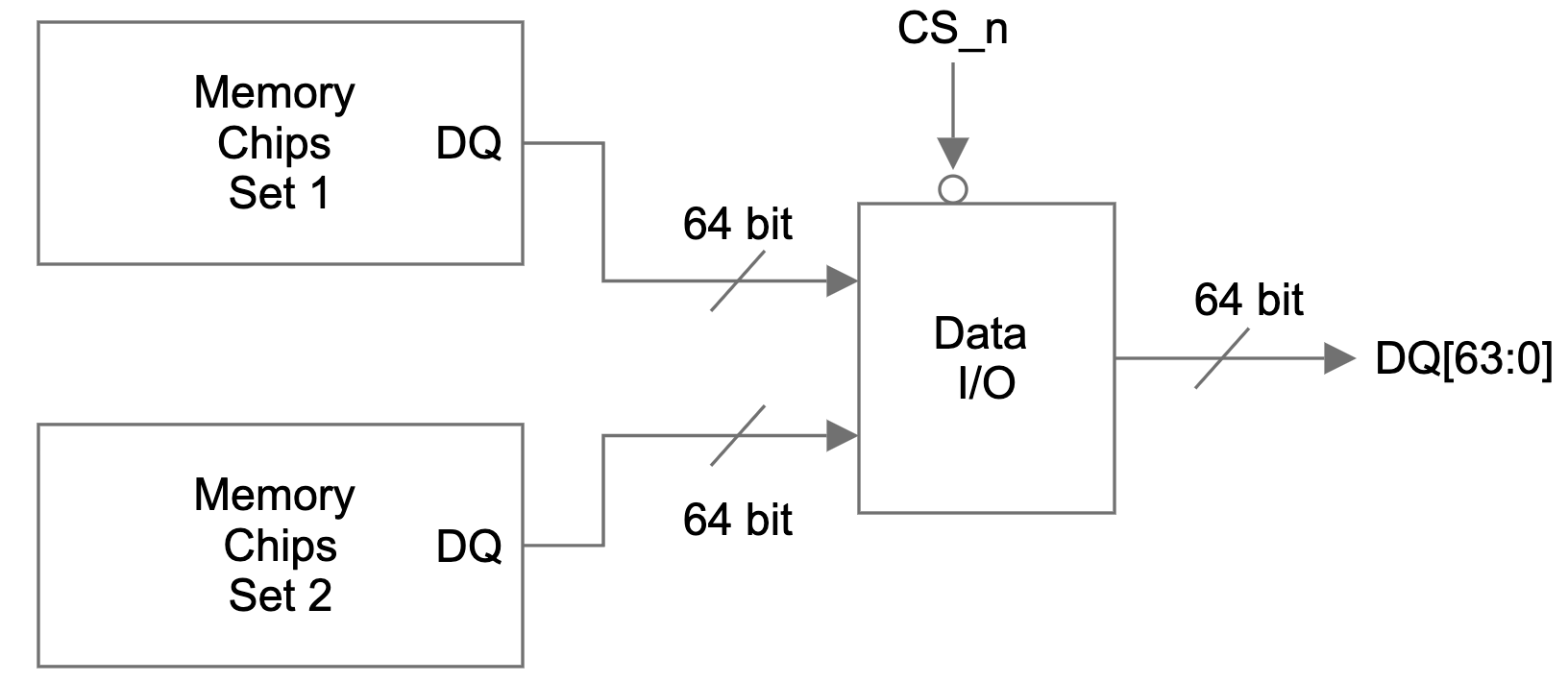
Figure 1 is a simplified view of the DQ signal flow on a dual-rank memory module. There are two identical sets of memory chips: set 1 and set 2. The 64-bit data I/O signals of each memory set are connected to a data I/O module. A single bit chip select (CS_n) signal controls which set of memory chips is accessed and the data I/O signals of the selected set will be connected to the DQ pins of the memory module.
Figure 1: DQ signal path on a dual rank memory module
Dual-rank and quad-rank memory modules double or quadruple the memory capacity on a module, within the existing memory technology. Even though only one rank can be accessed at a time, the other ranks are not sitting idle. Multi-rank memory modules use a process called rank interleaving, where the ranks that are not accessed go through their refresh cycles in parallel. This pipelined process reduces memory response time, as soon as the previous rank completes data transmission, the next rank can start its transmission.
On the other hand, there is some I/O latency penalty with multi-rank memory modules, since memory controllers need additional clock cycles to move from one rank to another. The overall latency performance difference between single rank and multi-rank memories depend heavily on the type of application.
In addition, because there are less memory chips on each module, single-rank modules produce less heat and are less likely to fail.
Memory depth and width
The capacity of each memory chip, or device, is defined as memory depth x memory width. Memory width refers to the width of the data bus, i.e. the number of DQ lines of each memory chip.
The width of memory chips are standard, they are either x4, x8 or x16. From here, we can calculate how many memory chips are in a 64-bit wide single rank memory. For example, with x4 memory chips, we will need 16 pieces (64 ÷ 4 = 16); and with x8 memory chips, we will only need 8 of them.
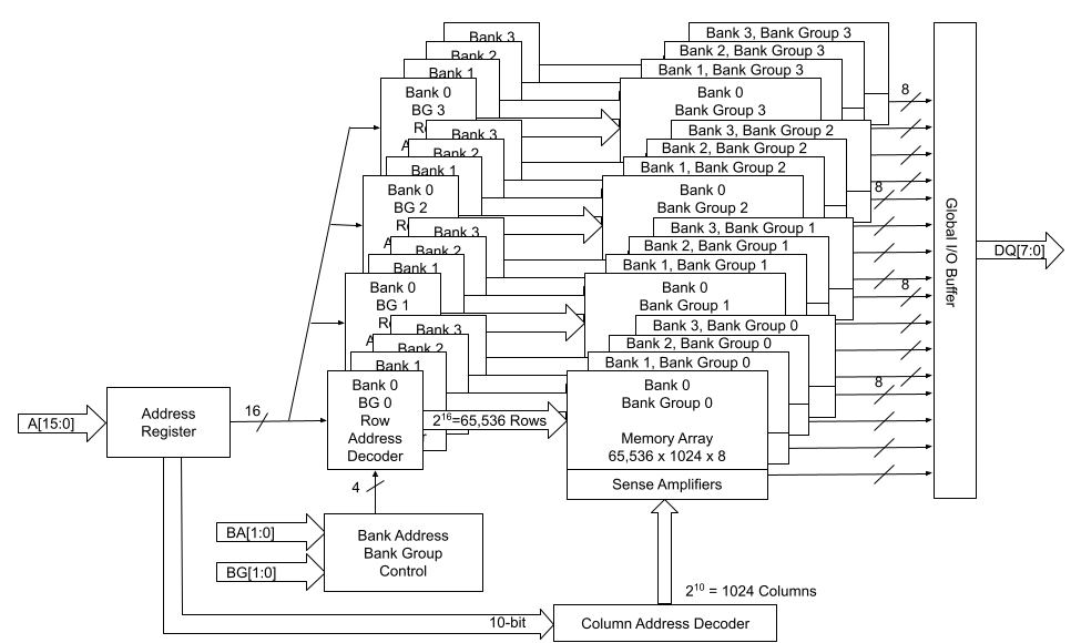
Let’s look at the following two high-level block diagrams of 1Gbx8 and 2Gbx4 memory chips. The total memory capacity for both of them is 8Gb. Figure 2 describes the 1Gb x8 configuration, and Figure 3 describes the 2Gbx4 configuration. With DDR4, both x4 and x8 devices have 4 groups of 4 banks. x16 devices have 2 groups of 4 banks.
We can think of each memory chip as a library. Within that library, there are four bank groups, which are the four floors of the library. On each floor, there are four shelves, each shelf is similar to one of the banks. And we can locate each one of the memory cells by its row and column addresses, just like the library book call numbers. Within each bank, the row address MUX activates a line in the memory array through the Row address latch and decoder, based on the given row address. This line is also called the word line. When a word line is activated, the data on the word line is loaded on to the sense amplifiers. Subsequently, the column decoder accesses the data on the sense amplifier based on the given column address.
Figure 2: 1Gbx8 block diagram
The capacity, or density of a memory chip is calculated as:
Memory Depth = Number of Rows * Number of Columns * Number of Banks
Total Memory Capacity = Memory Depth * Memory Width
In the example of a 1Gbx8 device as shown in Figure 2 above:
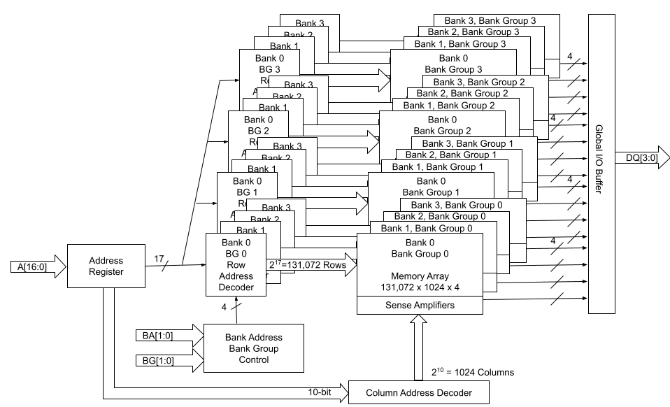
Figure 3 describes the function block diagram of a 2 Gb x 4 device.
Figure 3: 2Gbx4 Block Diagram
Number of Row Address Bits = 17
Total Number of Rows = 2 ^ 17 = 131072
Number of Column Address Bits = 10
Total Number of Columns = 2 ^ 10 = 1024
And the calculation goes:
Memory Depth = 131072 * 1024 * 16 = 2Gb
Total Memory Capacity = 2Gb* 4 = 8Gb
Memory module capacity
Memory rank and memory width determine how many memory devices are needed on each memory module.
A 64-bit DDR4 module with ECC support has a total of 72 bits for the data bus. Of the 72 bits, 8 bits are used for ECC. It would require a total of 18 x4 memory devices for a single rank module. Each memory device would supply 4 bits, and the total number of bits with 18 devices is 72 bits. For a dual rank module, we would need to double the amount of memory devices to 36.
If each x4 memory device has a memory capacity of 8Gb, a single rank module with 16 + 2 (ECC) devices would have 16GB module capacity.
8Gb * 16 = 128Gb = 16GB
And a dual rank ECC module with 36 8Gb (2Gb x 4) devices would have 32GB module capacity.
8Gb * 32 = 256Gb = 32GB
If the memory devices are x8, a 64-bit DDR4 module with ECC support would require a total of 9 x8 memory devices for a single rank module, and 18 x8 memory devices for a dual rank memory module. If each of these x8 memory devices has a memory capacity of 8Gb, a single rank module would have 8GB module capacity.
8Gb * 8 = 64Gb = 8GB
A dual rank ECC module with 18 8Gb (1Gb x 8) devices would have 16GB module capacity.
8Gb * 16 = 128Gb = 16GB
Notice that within the same memory device technology, for example 8Gb in our example, higher memory module capacity is achieved through using x4 device width, or dual-rank, or even quad-rank.
ACTIVATE timing and DRAM page sizes
Memory device width, whether it is x4, x8 or x16, also has an effect on memory timing parameters such as tFAW.
tFAW refers to Four Active Window time. It specifies a timing window within which four ACTIVATE commands can be issued. An ACTIVATE command is issued to open a row within a bank. In the block diagrams above we can see that each bank has its own set of sense amplifiers, thus one row can remain active per bank. A memory controller can issue four back-to-back ACTIVATE commands, but once the fourth ACTIVATE is done, the fifth ACTIVATE cannot be issued until the tFAW window expires.
The table below lists out the tFAW window lengths assigned to various DDR4 speeds and page sizes. Notice that under the same DDR4 speed, the bigger the page size, the longer the tFAW window is. For example, DDR4-1600 has a tFAW window of 20ns with 1/2KB page size. This means that within a bank, once a command to open a first row is issued, the controller must wait for 20ns, or 16 clock cycles (CK) before a command to open a fifth row can be issued.
The JEDEC memory standard specification for DDR4 tFAW timing varies by page sizes: 1/2KB, 1KB and 2KB.
Symbol
DDR4-1600
DDR4-1866
DDR4-2133
DDR4-2400
Four ACTIVATE windows for 1/2KB page size (minimum)
tFAW (1/2KB)
greater of 16CK or 20ns
greater of 16CK or 17ns
greater of 16CK or 15ns
greater of 16CK or 13ns
Four ACTIVATE windows for 1KB page size (minimum)
tFAW (1KB)
greater of 20CK or 25ns
greater of 20CK or 23ns
greater of 20CK or 21ns
greater of 20CK or 21ns
Four ACTIVATE windows for 2KB page size (minimum)
tFAW (2KB)
greater of 28CK or 35ns
greater of 28CK or 30ns
greater of 28CK or 30ns
greater of 28CK or 30ns
What is the relationship between page sizes and memory device width? Since we briefly compared two 8Gb memory devices earlier, it makes sense to take another look at those two in terms of page sizes.
Page size is the number of bits loaded into the sense amplifiers when a row is activated. Therefore page size is directly related to the number of bits per row, or number of columns per row.
Page Size = Number of Columns * Memory Device Width = 1024 * Memory Device Width
The table below shows the page sizes for each device width:
Device Width
Page Size (Kb)
Page Size (KB)
x4
4 Kb
1/2 KB
x8
8 Kb
1 KB
x16
16 Kb
2 KB
Among the three device widths, x4 devices have the shortest tFAW timing limit, and x16 devices have the longest tFAW timing limit. The difference in tFAW specification has a negative timing performance impact on devices with higher device width.
An experiment with 2Rx4 and 2Rx8 DDR4 modules
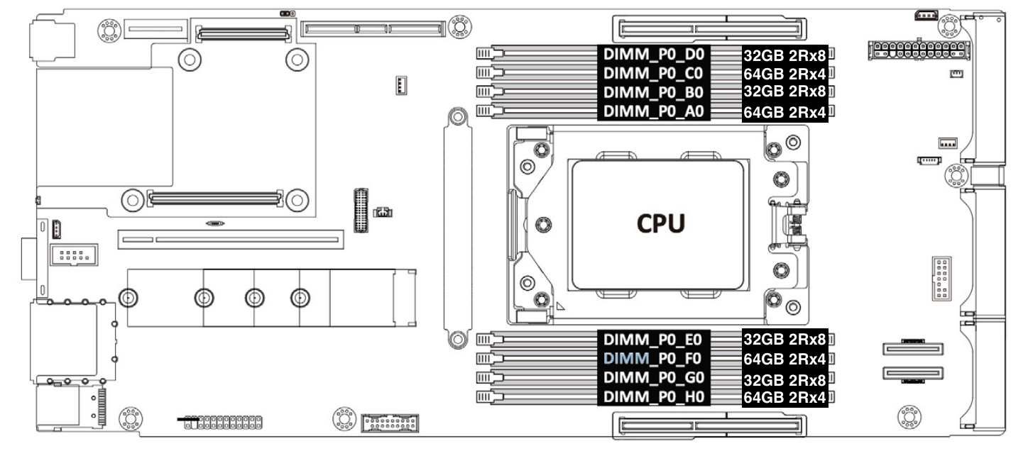
To quantify the impact on memory performance from different memory device widths, an experiment has been conducted on our Gen11 servers with AMD EPYC 7713 Rome CPU. The Rome CPU has 64 cores, supports 8 memory channels.
Our production Gen11 servers are configured with 1 DIMM populated in each memory channel. In order to achieve 6GB/core memory per core ratio, the total memory for the Gen11 system is 64 core * 6 GB/core = 384 GB. This is achieved by installing four pieces of 32GB 2Rx8 and four pieces of 64GB 2Rx4 memory modules.
Figure 5: Gen11 server memory configuration
To compare the bandwidth performance difference between 2Rx4 and 2Rx8 DDR4 modules, two test cases are needed. One with all 2Rx4 DDR4 modules, and another one with 2Rx8 DDR4 modules. Each test case populates eight pieces of 32GB 32Mbps DDR4 RDIMM memories in each memory channel (1DPC). As shown in the table below, the difference between the set up of the two test cases is: case A tests 2Rx4 memory modules, and case B tests 2Rx8 memory modules.
Test case
Number of DIMMs
Memory vendor
Part number
Memory size
Memory speed
Memory organization
A
8
Samsung
M393A4G43BB4-CWE
32GB
3200 MT/s
2Rx8
B
8
Samsung
M393A4K40EB3-CWECQ
32GB
3200 MT/s
2Rx4
Memory Latency Checker results
Memory Latency Checker is an Intel developed synthetic benchmarking tool. It measures memory latency and bandwidth, and how they vary with workloads of different read/write ratios, as well as stream triad. Stream triad is a memory benchmark workload that contains three operations: it first multiples a large 1D array with a scalar, then adds it to a second array, and assigns it to a third array.
2Rx8 32GB bandwidth (MB/s)
2Rx4 32GB bandwidth (MB/s)
Percentage difference
All reads
173,287
173,650
0.21%
3:1 reads-writes
154,593
156,343
1.13%
2:1 reads-writes
151,660
155,289
2.39%
1:1 reads-writes
146,895
151,199
2.93%
Stream-triad like
156,273
158,710
1.56%
The bandwidth performance difference in the All reads test case is not very significant, only 0.21%.
As the amount of writes increase, from 25% (3:1 reads-writes) to 50% (1:1 reads-writes), the bandwidth performance differences between test case A and test case B increase from 1.13% to 2.93%.
LMBench Results
LMBench is another synthetic benchmarking tool often used to study bandwidth performances of memory. Our LMBench bw_mem tests results are comparable to the results obtained from the MLC benchmark test.
2Rx8 32GB bandwidth (MB/s)
2Rx4 32GB bandwidth (MB/s)
Percentage difference
Read
170,285
173,897
2.12%
Write
73,179
76,019
3.88%
Read then write
72,804
74,926
2.91%
Copy
50,332
51,776
2.87%
The biggest bandwidth performance difference is with Write workload. The 2Rx4 test case has 3.88% higher write bandwidth than the 2Rx8 test case.
Summary
Memory organization and memory width has a slight effect on memory bandwidth performance. The difference is most obvious in write-heavy workloads than read-heavy workloads. But even in write-heavy workloads, the difference is less than 4% according to our benchmark tests.
Memory modules with x4 width require twice the number of memory devices on the memory module, as compared to memory modules with x8 width of the same capacity. More memory devices would consume more power. According to Micron’s measurement data, 2Rx8 32GB memory modules using 16Gb devices consume 31% less power than 2Rx4 32GB memory modules using 8Gb devices. The substantial power saving of using x8 memory modules may outweigh the slight bandwidth performance impact.
Our Gen11 servers are configured with a mix of 2Rx4 and 2Rx8 DDR4 modules. For our future generations, we may consider using 2Rx8 memory where possible, in order to reduce overall system power consumption, with minimal impact to bandwidth performance.
In previous posts we wrote about our configuration distribution system Quicksilver and the story of migrating its storage engine to RocksDB. This solution proved to be fast, resilient and stable. During the migration process, we noticed that Quicksilver memory consumption was unexpectedly high. After our investigation we found out that the root cause was a default memory allocator that we used. Switching memory allocator improved service memory consumption by almost three times.
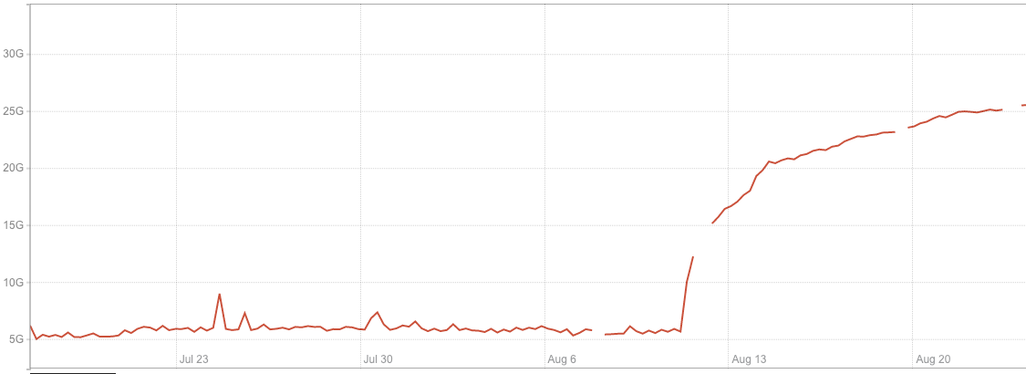
Unexpected memory growth
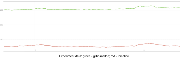
After migrating to RocksDB, the memory used by the application increased significantly. Also, the way memory was growing over time looked suspicious. It was around 15GB immediately after start and then was steadily growing for multiple days, until stabilizing at around 30GB. Below, you can see a memory consumption increase after migrating one of our test instances to RocksDB.
We started our investigation with heap profiling with the assumption that we had a memory leak somewhere and found that heap size was almost three times less than the RSS value reported by the operating system. So, if our application does not actually use all this memory, it means that memory is ‘lost’ somewhere between the system and our application, which points to possible problems with the memory allocator.
We have multiple services running with the tcmalloc allocator, so in order to test our hypothesis, we ran a test with TCMalloc on a couple of instances. The test showed significant improvement in memory usage. So why did this happen? We’ll dig into memory allocator internals to understand the issue.
glibc malloc
Let’s begin with a high level view of glibc’s malloc design. malloc uses a concept called an arena. An arena is a contiguous block of memory obtained from the system. An important part of glibc malloc design is that it expects developers to free memory in a reverse order of allocation, otherwise a lot of memory will be ‘locked’, and never returned to the system. Let’s see what it means on practise:
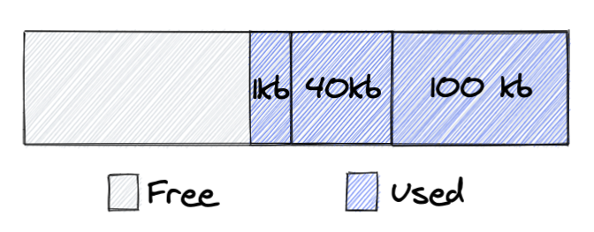
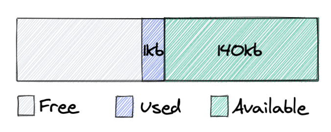
In the picture, you can see an arena, from which we allocated three chunks of memory: 100kb, 40kb, 1kb. Next, the application frees the chunks with sizes of 40kb and 100kb:
Before we go further, let me explain the terminology I use here and what each type of memory means:
Free – this is virtual memory of a process, not backed by physical memory, and corresponds to the VIRT parameter of the top/ps command.
Used – memory used by the application, backed by physical memory, contributes to the RES parameter of the top/ps command.
Available – memory held by the allocator, backed by physical memory. The allocator can either return this memory to the OS, and it would become ‘Free’ or later reuse it to satisfy application requests. From a system perspective, this memory is still held by the application. Available + Used = RES.
So we see that memory which was used by the application changed state to Available, and it’s not returned to the operating system. This is because malloc can only return memory from the top of the heap, and in the case above we have a chunk of memory that blocks 140kb from being released back to the system. As soon as we release this 1kb object, all memory can be returned to the system.
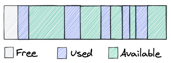
Let’s go further with our simple example, if our application allocates/frees memory without keeping malloc’s design in mind, after a while we will see roughly following picture:
Here we see one of the main problems that all allocators try to solve: memory fragmentation. We have some chunks used by the application, but a lot of the memory is not used at the moment. And since it’s not returned to the system, other services can’t use this memory either. Malloc implements several mechanisms to decrease memory fragmentation, but it’s a problem that all allocators have, and how bad this problem is depends on a lot of factors: allocator design, workload, settings, etc.
OK, so the problem is clear, memory fragmentation, but why did it lead to such high memory usage? To understand that, let’s take a step back and consider how malloc works for highly concurrent multithreaded applications.
To allocate a chunk of memory from an arena, a thread should acquire an exclusive lock for that arena. When an application has multiple threads this would create lock contention and poor performance for multithreaded services. To handle this situation malloc creates several arenas, using the following logic:
A thread tries to get a chunk of memory from an arena it used last time, in order to do that it acquires an exclusive lock for the arena
If the lock is held by another thread, it tries the next arena
If all arenas were locked it creates a new arena and uses memory from it
There is a limit on the number of arenas – eight arenas per core
Normally, our service has around 25 threads, and we have seen 60-80 arenas allocated by malloc using the logic above.
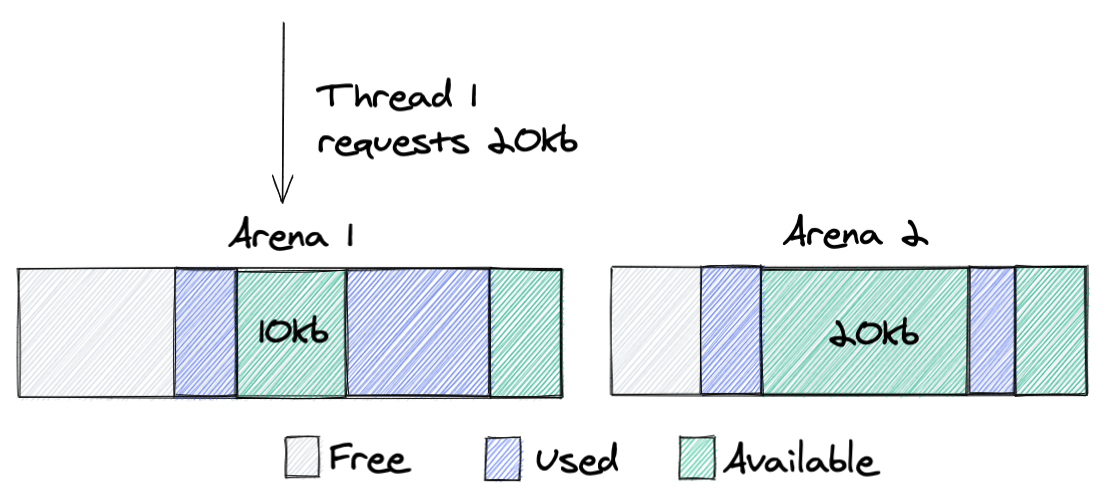
And this is a place where the fragmentation problem magnifies and leads to huge memory waste. All arenas are independent of each other and memory can never move from one arena to another. Why is that bad? Let’s take a look at the following example:
Here, we can see that Thread 1 requests 20kb of memory from Arena 1; as I’ve written before, malloc tries to allocate memory from the same arena it’s used before. Since Arena 1 still has enough free memory, Thread 1 will get a block from it, which at the end will increase memory that the process takes from the system. Ideally, in this scenario, we would prefer to get this block of memory from Arena 2, since it has a chunk of that size available. However, due to the design this won’t happen.
The main point here: having multiple independent arenas improves the performance of multithreaded applications, by reducing lock contention, but the trade-off is that it increases memory fragmentation, since each memory request chooses the best fit fragment from an individual arena and not the best fit fragment overall.
Remember, I wrote that memory locked between used chunks can never be returned to the system? Actually, there is a way to do that, ‘malloc_trim’ is a function provided by glibc malloc, and it does exactly that. It goes through all the unused chunks and returns them to the system. The problem is that you need to explicitly call this function from your application. You might say: “Oh, wait, I remember that this function is sometimes called when you call the free function, I saw it in the man page.” No, that never happens, it’s a bug in the man page that has existed for more than 15 years, which is now finally fixed!
Let’s now discuss what options we have to improve the memory consumption of glibc malloc. Here are a couple of useful strategies to try out:
The first thing you would find on the Internet is to reduce MALLOC_ARENA_MAX to a lower value, usually 2. This setting limits the number of arenas malloc would create per core. The fewer arenas we have the better the memory reuse, hence lower fragmentation, but at the same time it would increase lock contention.
Calling malloc_trim from time to time. This function goes through all arenas one at a time, it locks the arena and releases all locked chunks back to the system. This at the end increases lock contention and will execute a lot of syscalls to return memory and later would lead to more page faults and again worse performance.
M_MMAP_THRESHOLD. All allocations higher than this parameter would use the mmap syscall, and would not take memory from the arena directly. That means that memory allocated with this approach would never be locked between used chunks of memory and can always be returned to the system. It solves the fragmentation problem for large chunks, so only small chunks would be locked. The trade-off here is that each such allocation would execute an expensive syscall. And there is a system limit that caps the maximum number of chunks allocated with mmap.
Short summary: multiple arenas cause higher memory fragmentation that can lead to 2-3x higher memory consumption.
TCMalloc
While glibc malloc was designed for single-threaded applications and later optimized for multithreaded services, TCMalloc was built for multithreading at the beginning. Let’s take a look at how it tries to solve the problems we just talked about. The TCMalloc design is more complex, so if you want to understand the details I recommend reading the official design page. Here is a high level view of its design:
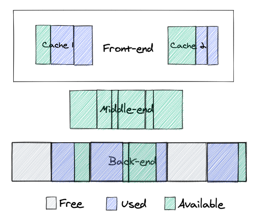
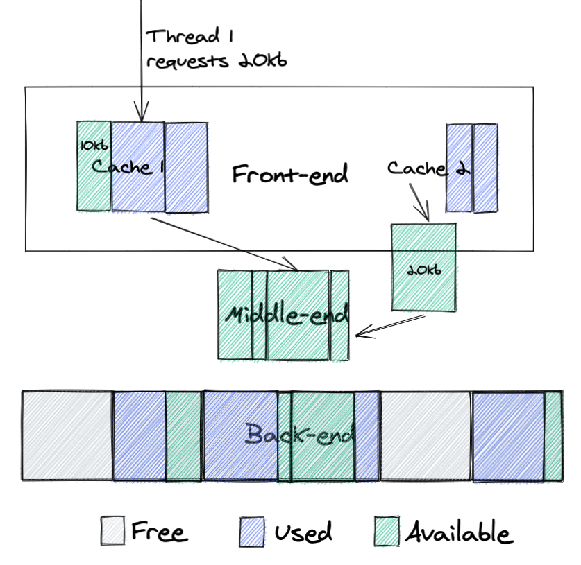
Here we can see 3 main parts of TCMalloc design:
Back-end: allocates big chunks of memory from the system, returns these chunks back to the operating system when they are not needed and also serves big allocation requests.
Front-end: serves allocation requests, there is one cache per core.
Middle-end: this is a core part of the TCMalloc design, which helps to significantly reduce fragmentation for multithreaded applications. It populates caches and returns unused memory to the back-end, but most importantly it can move memory from one cache to another, dramatically improving memory reuse.
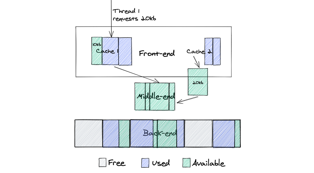
Let’s look how it works on the example that we showed for malloc:
Here we see the following:
Cache 2 has a chunk of memory that it doesn’t need, so it returns it to the middle-end
Thread 1 requests 20kb of memory from cache 1
Cache 1 doesn’t have a chunk of memory of that size, so it requests this memory from middle-end, where it can reuse memory from cache 2
This design dramatically improves memory reuse. If memory was freed by one thread it can be moved to the middle-end and later reused by other threads.
Conclusion
The main goal of this post is to make people aware of the importance of the choice of memory allocator. After deploying TCMalloc, we decreased memory usage by 2.5 times.
Usage of an allocator which is not optimal for a workload can cause a huge waste of memory. If you have a long-running application with a lot of threads and care about memory usage then glibc malloc is probably not your choice. Allocators that are designed for multithreaded services, like TCMalloc, jemalloc and others can provide much better memory utilization. So be conscious of this factor and go and check how much memory your application wastes.
The collective thoughts of the interwebz
Manage Consent
To provide the best experiences, we use technologies like cookies to store and/or access device information. Consenting to these technologies will allow us to process data such as browsing behavior or unique IDs on this site. Not consenting or withdrawing consent, may adversely affect certain features and functions.
Functional
Always active
The technical storage or access is strictly necessary for the legitimate purpose of enabling the use of a specific service explicitly requested by the subscriber or user, or for the sole purpose of carrying out the transmission of a communication over an electronic communications network.
Preferences
The technical storage or access is necessary for the legitimate purpose of storing preferences that are not requested by the subscriber or user.
Statistics
The technical storage or access that is used exclusively for statistical purposes.The technical storage or access that is used exclusively for anonymous statistical purposes. Without a subpoena, voluntary compliance on the part of your Internet Service Provider, or additional records from a third party, information stored or retrieved for this purpose alone cannot usually be used to identify you.
Marketing
The technical storage or access is required to create user profiles to send advertising, or to track the user on a website or across several websites for similar marketing purposes.