Encryption can protect data at rest and data in transit, but does nothing for data in use. What we have are secure enclaves. I’ve written about this before:
Almost all cloud services have to perform some computation on our data. Even the simplest storage provider has code to copy bytes from an internal storage system and deliver them to the user. End-to-end encryption is sufficient in such a narrow context. But often we want our cloud providers to be able to perform computation on our raw data: search, analysis, AI model training or fine-tuning, and more. Without expensive, esoteric techniques, such as secure multiparty computation protocols or homomorphic encryption techniques that can perform calculations on encrypted data, cloud servers require access to the unencrypted data to do anything useful.
Fortunately, the last few years have seen the advent of general-purpose, hardware-enabled secure computation. This is powered by special functionality on processors known as trusted execution environments (TEEs) or secure enclaves. TEEs decouple who runs the chip (a cloud provider, such as Microsoft Azure) from who secures the chip (a processor vendor, such as Intel) and from who controls the data being used in the computation (the customer or user). A TEE can keep the cloud provider from seeing what is being computed. The results of a computation are sent via a secure tunnel out of the enclave or encrypted and stored. A TEE can also generate a signed attestation that it actually ran the code that the customer wanted to run.
Secure enclaves are critical in our modern cloud-based computing architectures. And, of course, they have vulnerabilities:
The most recent attack, released Tuesday, is known as TEE.fail. It defeats the latest TEE protections from all three chipmakers. The low-cost, low-complexity attack works by placing a small piece of hardware between a single physical memory chip and the motherboard slot it plugs into. It also requires the attacker to compromise the operating system kernel. Once this three-minute attack is completed, Confidential Compute, SEV-SNP, and TDX/SDX can no longer be trusted. Unlike the Battering RAM and Wiretap attacks from last month—which worked only against CPUs using DDR4 memory—TEE.fail works against DDR5, allowing them to work against the latest TEEs.
Yes, these attacks require physical access. But that’s exactly the threat model secure enclaves are supposed to secure against.
Apple has introduced a new hardware/software security feature in the iPhone 17: “Memory Integrity Enforcement,” targeting the memory safety vulnerabilities that spyware products like Pegasus tend to use to get unauthorized system access. From Wired:
In recent years, a movement has been steadily growing across the global tech industry to address a ubiquitous and insidious type of bugs known as memory-safety vulnerabilities. A computer’s memory is a shared resource among all programs, and memory safety issues crop up when software can pull data that should be off limits from a computer’s memory or manipulate data in memory that shouldn’t be accessible to the program. When developers—even experienced and security-conscious developers—write software in ubiquitous, historic programming languages, like C and C++, it’s easy to make mistakes that lead to memory safety vulnerabilities. That’s why proactive tools like special programming languages have been proliferating with the goal of making it structurally impossible for software to contain these vulnerabilities, rather than attempting to avoid introducing them or catch all of them.
[…]
With memory-unsafe programming languages underlying so much of the world’s collective code base, Apple’s Security Engineering and Architecture team felt that putting memory safety mechanisms at the heart of Apple’s chips could be a deus ex machina for a seemingly intractable problem. The group built on a specification known as Memory Tagging Extension (MTE) released in 2019 by the chipmaker Arm. The idea was to essentially password protect every memory allocation in hardware so that future requests to access that region of memory are only granted by the system if the request includes the right secret.
Arm developed MTE as a tool to help developers find and fix memory corruption bugs. If the system receives a memory access request without passing the secret check, the app will crash and the system will log the sequence of events for developers to review. Apple’s engineers wondered whether MTE could run all the time rather than just being used as a debugging tool, and the group worked with Arm to release a version of the specification for this purpose in 2022 called Enhanced Memory Tagging Extension.
To make all of this a constant, real-time defense against exploitation of memory safety vulnerabilities, Apple spent years architecting the protection deeply within its chips so the feature could be on all the time for users without sacrificing overall processor and memory performance. In other words, you can see how generating and attaching secrets to every memory allocation and then demanding that programs manage and produce these secrets for every memory request could dent performance. But Apple says that it has been able to thread the needle.
The government of China has accused Nvidia of inserting a backdoor into their H20 chips:
China’s cyber regulator on Thursday said it had held a meeting with Nvidia over what it called “serious security issues” with the company’s artificial intelligence chips. It said US AI experts had “revealed that Nvidia’s computing chips have location tracking and can remotely shut down the technology.”
Cloudflare’s network spans more than 330 cities in over 120 countries, serving over 60 million HTTP requests per second and 39 million DNS queries per second on average. These numbers will continue to grow, and at an accelerating pace, as will Cloudflare’s infrastructure to support them. While we can continue to scale out by deploying more servers, it is also paramount for us to develop and deploy more performant and more efficient servers.
At the heart of each server is the processor (central processing unit, or CPU). Even though many aspects of a server rack can be redesigned to improve the cost to serve a request, CPU remains the biggest lever, as it is typically the primary compute resource in a server, and the primary enabler of new technologies.
The following table is a summary of the specification of the AMD EPYC 7713 CPU in our Gen 11 server against the three CPU candidates, one from each variant of the 4th generation AMD EPYC Processors architecture:
* AMD EPYC 7713 all core boost clock is based on Cloudflare production data, not the official specification from AMD
cf_benchmark
Readers may remember that Cloudflare introduced cf_benchmark when we evaluated Qualcomm’s ARM chips, using it as our first pass benchmark to shortlist AMD’s Rome CPU for our Gen 10 servers and to evaluate our chosen ARM CPU Ampere Altra Max against AWS Graviton 2. Likewise, we ran cf_benchmark against the three candidate CPUs for our 12th Gen servers: AMD EPYC 9654 (Genoa), AMD EPYC 9754 (Bergamo), and AMD EPYC 9684X (Genoa-X). The majority of cf_benchmark workloads are compute bound, and given more cores or higher CPU frequency, they score better. The graph and the table below show the benchmark performance comparison of the three CPU candidates with Genoa 9654 as the baseline, where > 1.00x indicates better performance.
Genoa 9654 (baseline)
Bergamo 9754
Genoa-X 9684X
openssl_pki
1.00x
1.16x
1.01x
openssl_aead
1.00x
1.20x
1.01x
luajit
1.00x
0.86x
1.00x
brotli
1.00x
1.11x
0.98x
gzip
1.00x
0.87x
1.01x
go
1.00x
1.09x
1.00x
Bergamo 9754 with 128 cores scores better in openssl_pki, openssl_aead, brotli, and go benchmark suites, and performs less favorably in luajit and gzip benchmark suites. Genoa-X 9684X (with significantly more L3 cache) doesn’t offer a significant boost in performance for these compute-bound benchmarks.
These benchmarks are representative of some of the common workloads Cloudflare runs, and are useful in identifying software scaling issues, system configuration bottlenecks, and the impact of CPU design choices on workload-specific performance. However, the benchmark suite is not an exhaustive list of all workloads Cloudflare runs in production, and in reality, the workloads included in the benchmark suites are almost certainly not the exclusive workload running on the CPU. In short, though benchmark results can be informative, they do not represent a good indication of production performance when a mix of these workloads run on the same processor.
Performance simulation
To get an early indication of production performance, Cloudflare has an internal performance simulation tool that exercises our software stack to fetch a fixed asset repeatedly. The simulation tool can be configured to fetch a specified fixed-size asset and configured to include or exclude services like WAF or Workers in the request path. Below, we show the simulated performance between the three CPUs for an asset size of 10 KB, where >1.00x indicates better performance.
Milan 7713
Genoa 9654
Bergamo 9754
Genoa-X 9684X
Lab simulation performance multiplier
1.00x
2.20x
1.95x
2.75x
Based on these results, Bergamo 9754, which has the highest core count, but smallest L3 cache per core, is least performant among the three candidates, followed by Genoa 9654. The Genoa-X 9684X with the largest L3 cache per core is the most performant. This data suggests that our software stack is very sensitive to L3 cache size, in addition to core count and CPU frequency. This is interesting and worth a deep dive into a sensitivity analysis of our workload against a few (high level) CPU design points, especially core scaling, frequency scaling, and L2/L3 cache sizes scaling.
Sensitivity analysis
Core sensitivity
Number of cores is the headline specification that practically everyone talks about, and one of the easiest improvements CPU vendors can make to increase performance per socket. The AMD Genoa 9654 has 96 cores, 50% more than the 64 cores available on the AMD Milan 7713 CPUs that we used in our Gen 11 servers. Is more always better? Does Cloudflare’s primary workload scale with core count and effectively utilize all available cores?
The figure and table below shows the result of a core scaling experiment performed on an AMD Genoa 9654 configured with 96 cores, 80 cores, 64 cores, and 48 cores, which was done by incrementally disabling 2x CCD (8 cores/CCD) at each step. The result is GREAT, as Cloudflare’s simulated primary workload scales linearly with core count on AMD Genoa CPUs.
The chart below shows the result of sweeping the TDP of the AMD Genoa 9654 (in power determinism mode) from 240W to 400W. (Note: x-axis step size is not linear).
Cloudflare’s simulated primary workload continues to see incremental performance improvements up to the maximum configurable 400W, albeit at a less favorable perf/watt ratio.
Looking at TDP sensitivity data is a quick and easy way to identify if performance stagnates at some power point, but what does power sensitivity actually measure? There are several factors contributing to CPU power consumption, but let’s focus on one of the primary factors: dynamic power consumption. Dynamic power consumption is approximately CV2f, where C is the switched load capacitance, V is the regulated voltage, and f is the frequency. In modern processors like the AMD Genoa 9654, the CPU dynamically scales its voltage along with frequency, so theoretically, CPU dynamic power is loosely proportional to f3. In other words, measuring TDP sensitivity is measuring the frequency sensitivity of a workload. Does the data agree? Yes!
cTDP
All core boost frequency (GHz)
Perf (rps) / baseline
240
2.47
0.78x
280
2.75
0.87x
320
2.93
0.93x
340
3.13
0.97x
360
3.3
1.00x
380
3.4
1.03x
390
3.465
1.04x
400
3.55
1.05x
Frequency sensitivity
Instead of relying on an indirect measure through the TDP, let’s measure frequency sensitivity directly by sweeping the maximum boost frequency.
At above 3GHz, the data shows that Cloudflare’s primary workload sees roughly 2% incremental improvement for every 0.1GHz all core average frequency increment. We hit the 400W power cap at 3.545GHz. This is notably higher than the typical all core boost frequency that Cloudflare Gen 11 servers with AMD Milan 7713 at 2.7GHz see in production, or at 2.4GHz in our performance simulation, which is amazing!
L3 cache size sensitivity
What about L3 cache size sensitivity? L3 cache size is one of the primary design choices and major differences between the trio of Genoa, Bergamo, and Genoa-X. Genoa 9654 has 4 MB L3/core, Bergamo 9754 has 2 MB L3/core, and Genoa-X has 12 MB L3/core. L3 cache is the last and largest “memory” bank on-chip before having to access memory on DIMMs outside the chip that would take significantly more CPU cycles.
We ran an experiment on the Genoa 9654 to check how performance scales with L3 cache size. L3 cache size per core is reduced through MSR writes (but could also be done using Intel RDT) and L3 cache per core is increased by disabling physical cores in a CCD (which reduces the number of cores sharing the fixed size 32 MB L3 cache per CCD effectively growing the L3 cache per core). Below is the result of the experiment, where >1.00x indicates better performance:
L3 cache size increase vs baseline 4MB per core
0.25x
0.5x
0.75x
1x
1.14x
1.33x
1.60x
2.00x
rps/core / baseline
0.67x
0.78x
0.89x
1.00x
1.08x
1.15x
1.25x
1.31x
L3 cache miss rate per CCD
56.04%
39.15%
30.37%
23.55%
22.39%
19.73%
16.94%
14.28%
Even though the expectation was that the impact of a different L3 cache size gets diminished by the faster DDR5 and larger memory bandwidth, Cloudflare’s simulated primary workload is quite sensitive to L3 cache size. The L3 cache miss rate dropped from 56% with only 1 MB L3 per core, to 14.28% with 8 MB L3/core. Changing the L3 cache size by 25% affects the performance by approximately 11%, and we continue to see performance increase to 2x L3 cache size, though the performance increase starts to diminish when we get to 2x L3 cache per core.
Do we see the same behavior when comparing Genoa 9654, Bergamo 9754 and Genoa-X 9684X? We ran an experiment comparing the impact of L3 cache size, controlling for core count and all core boost frequency, and we also saw significant deltas. Halving the L3 cache size from 4 MB/core to 2 MB/core reduces performance by 24%, roughly matching the experiment above. However, increasing the cache 3x from 4 MB/core to 12 MB/core only increases performance by 25%, less than the indication provided by previous experiments. This is likely because the performance gain we saw on experiment result above could be partially attributed to less cache contention due to reduced number of cores based on how we set up the test. Nevertheless, these are significant deltas!
L3/core
2MB/core
4MB/core
12MB/core
Perf (rps) / baseline
0.76x
1x
1.25x
Putting it all together
The table below summarizes how each factor from sensitivity analysis above contributes to the overall performance gain. There are an additional 6% to 14% of unaccounted performance improvement that are contributed by other factors like larger L2 cache, higher memory bandwidth, and miscellaneous CPU architecture changes that improve IPC.
Milan
7713
Genoa
9654
Bergamo
9754
Genoa-X
9684X
Lab simulation performance multiplier
1x
2.2x
1.95x
2.75x
Performance multiplier due to Core scaling
1x
1.5x
2x
1.5x
Performance multiplier due to Frequency scaling
(*Note: Milan 7713 all core frequency is ~2.4GHz when running simulated workload at 100% CPU utilization)
1x
1.32x
1.21x
1.29x
Performance multiplier due to L3 cache size scaling
1x
1x
0.76x
1.25x
Performance multiplier due to other factors like larger L2 cache, higher memory bandwidth, miscellaneous CPU architecture changes that improve IPC
1x
1.11x
1.06x
1.14x
Performance evaluation in production
How do these CPU candidates perform with real-world traffic and an actual production workload mix? The table below summarizes the performance of the three CPUs in lab simulation and in production. Genoa-X 9684X continues to outperform in production.
In addition, the Gen 12 server equipped with Genoa-X offered outstanding performance but only consumed 1.5x more power per system than our Gen 11 server with Milan 7713. In other words, we see a 63% increase in performance per watt. Genoa-X 9684X provides the best TCO improvement among the 3 options, and was ultimately chosen as the CPU for our Gen 12 server.
Milan 7713
Genoa 9654
Bergamo 9754
Genoa-X 9684X
Lab simulation performance multiplier
1x
2.2x
1.95x
2.75x
Production performance multiplier
1x
2x
2.15x
2.45x
Production performance per watt multiplier
1x
1.33x
1.38x
1.63x
The Gen 12 server with AMD Genoa-X 9684X is the most powerful and the most power efficient server Cloudflare has built to date. It serves as the underlying platform for all the incredible services that Cloudflare offers to our customers globally, and will help power the growth of Cloudflare infrastructure for the next several years with improved cost structure.
Hardware engineers at Cloudflare work closely with our infrastructure engineering partners and externally with our vendors to design and develop world-class servers to best serve our customers.
Come join us at Cloudflare to help build a better Internet!
In the dynamic evolution of AI and cloud computing, the deployment of efficient and reliable hardware is critical. As we roll out our Gen 12 hardware across hundreds of cities worldwide, the challenge of maintaining optimal thermal performance becomes essential. This blog post provides a deep dive into the robust thermal design that supports our newest Gen 12 server hardware, ensuring it remains reliable, efficient, and cool (pun very much intended).
The importance of thermal design for hardware electronics
Generally speaking, a server has five core resources: CPU (computing power), RAM (short term memory), SSD (long term storage), NIC (Network Interface Controller, connectivity beyond the server), and GPU (for AI/ML computations). Each of these components can withstand different temperature limits based on their design, materials, location within the server, and most importantly, the power they are designed to work at. This final criteria is known as thermal design power (TDP).
The reason why TDP is so important is closely related to the first law of thermodynamics, which states that energy cannot be created or destroyed, only transformed. In semiconductors, electrical energy is converted into heat, and TDP measures the maximum heat output that needs to be managed to ensure proper functioning.
Back in December 2023, we talked about our decision to move to a 2U form factor, doubling the height of the server chassis to optimize rack density and increase cooling capacity. In this post, we want to share more details on how this additional space is being used to improve performance and reliability supporting up to three times more total system power.
Standardization
In order to support our multi-vendor strategy that mitigates supply chain risks ensuring continuity for our infrastructure, we introduced our own thermal specification to standardize thermal design and system performance. At Cloudflare, we find significant value in building customized hardware optimized for our unique workloads and applications, and we are very fortunate to partner with great hardware vendors who understand and support this vision. However, partnering with multiple vendors can introduce design variables that Cloudflare then controls for consistency within a hardware generation. Some of the most relevant requirements we include in our thermal specification are:
Ambient conditions: Given our globally distributed footprint with presence in over 330 cities, environmental conditions can vary significantly. Hence, servers in our fleet can experience a wide range of temperatures, typically ranging between 28 to 35°C. Therefore, our systems are designed and validated to operate with no issue over temperature ranges from 5 to 40°C (following the ASHRAE A3 definition).
Thermal margins: Cloudflare designs with clear requirements for temperature limits on different operating conditions, simulating peak stress, average workloads, and idle conditions. This allows Cloudflare to validate that the system won’t experience thermal throttling, which is a power management control mechanism used to protect electronics from high temperatures.
Fan failure support to increase system reliability: This new generation of servers is 100% air cooled. As such, the algorithm that controls fan speed based on critical component temperature needs to be optimized to support continuous operation over the server life cycle. Even though fans are designed with a high (up to seven years) mean time between failure (MTBF), we know fans can and do fail. Losing a server’s worth of capacity due to thermal risks caused by a single fan failure is expensive. Cloudflare requires the server to continue to operate with no issue even in the event of one fan failure. Each Gen 12 server contains four axial fans providing the extra cooling capacity to prevent failures.
Maximum power used to cool the system: Because our goal is to serve more Internet traffic using less power, we aim to ensure the hardware we deploy is using power efficiently. Great thermal management must consider the overall cost of cooling relative to the total system power input. It is inefficient to burn power consumption on cooling instead of compute. Thermal solutions should look at the hardware architecture holistically and implement mechanical modifications to the system design in order to optimize airflow and cooling capacity before considering increasing fan speed, as fan power consumption proportionally scales to the cube of its rotational speed. (For example, running the fans at twice (2x) the rotational speed would consume 8x more power,)
System layout
Placing each component strategically within the server will also influence the thermal performance of the system. For this generation of servers, we made several internal layout decisions, where the final component placement takes into consideration optimal airflow patterns, preventing pre-heated air from affecting equipment in the rear end of the chassis.
Bigger and more powerful fans were selected in order to take advantage of the additional volume available in a 2U form factor. Growing from 40 to 80 millimeters, a single fan can provide up to four times more airflow. Hence, bigger fans can run at slower speeds to provide the required airflow to cool down the same components, significantly improving power efficiency.
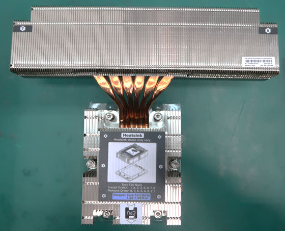
The Extended Volume Air Cooled (EVAC) heatsink was optimized for Gen 12 hardware, and is designed with increased surface area to maximize heat transfer. It uses heatpipes to move the heat effectively away from the CPU to the extended fin region that sits immediately in front of the fans as shown in the picture below.
EVAC heatsink installed in one of our Gen 12 servers. The extended fin region sits right in front of the axial fans. (Photo courtesy of vendor.)
The combination of optimized heatsink design and selection of high-performing fans is expected to significantly reduce the power used for cooling the system. These savings will vary depending on ambient conditions and system stress, but under a typical stress scenario at 25°C ambient temperature, power savings could be as much as 50%.
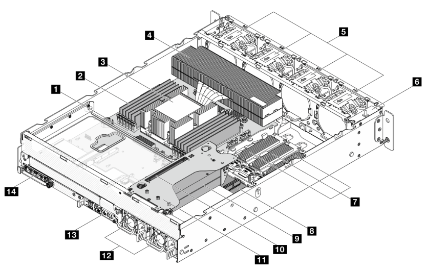
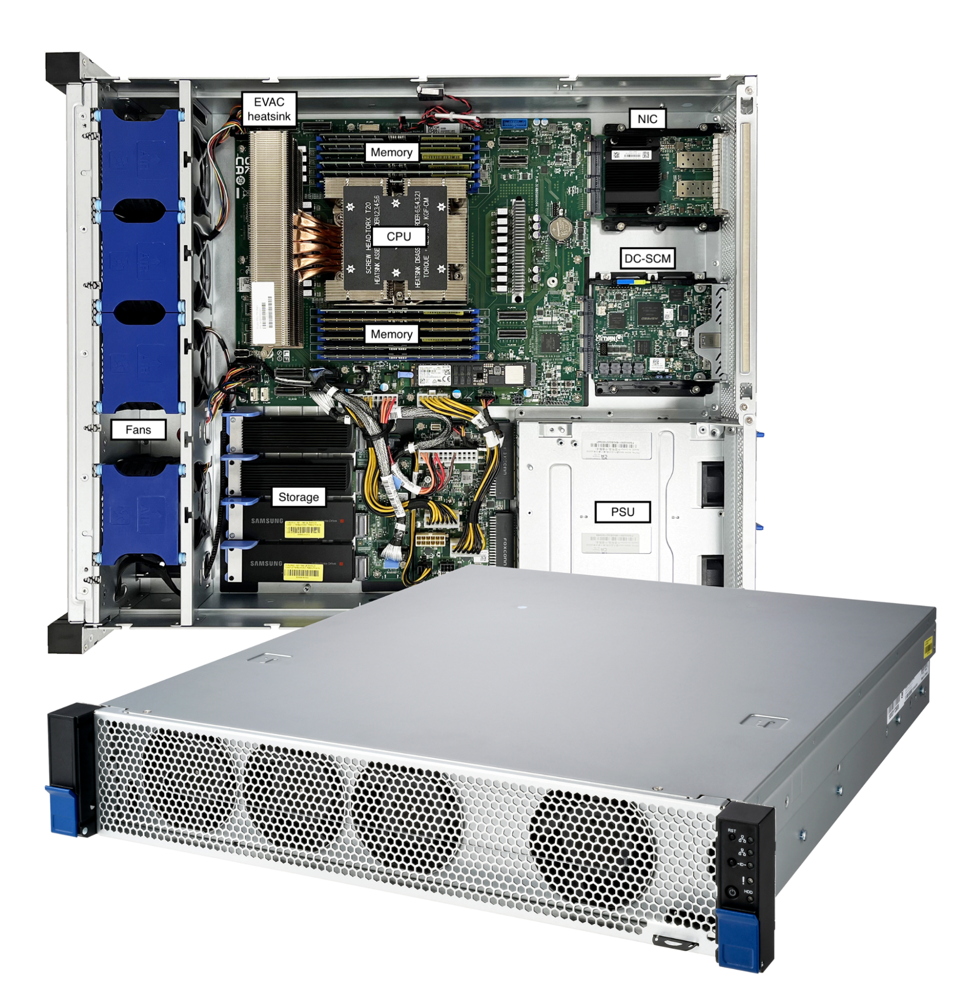
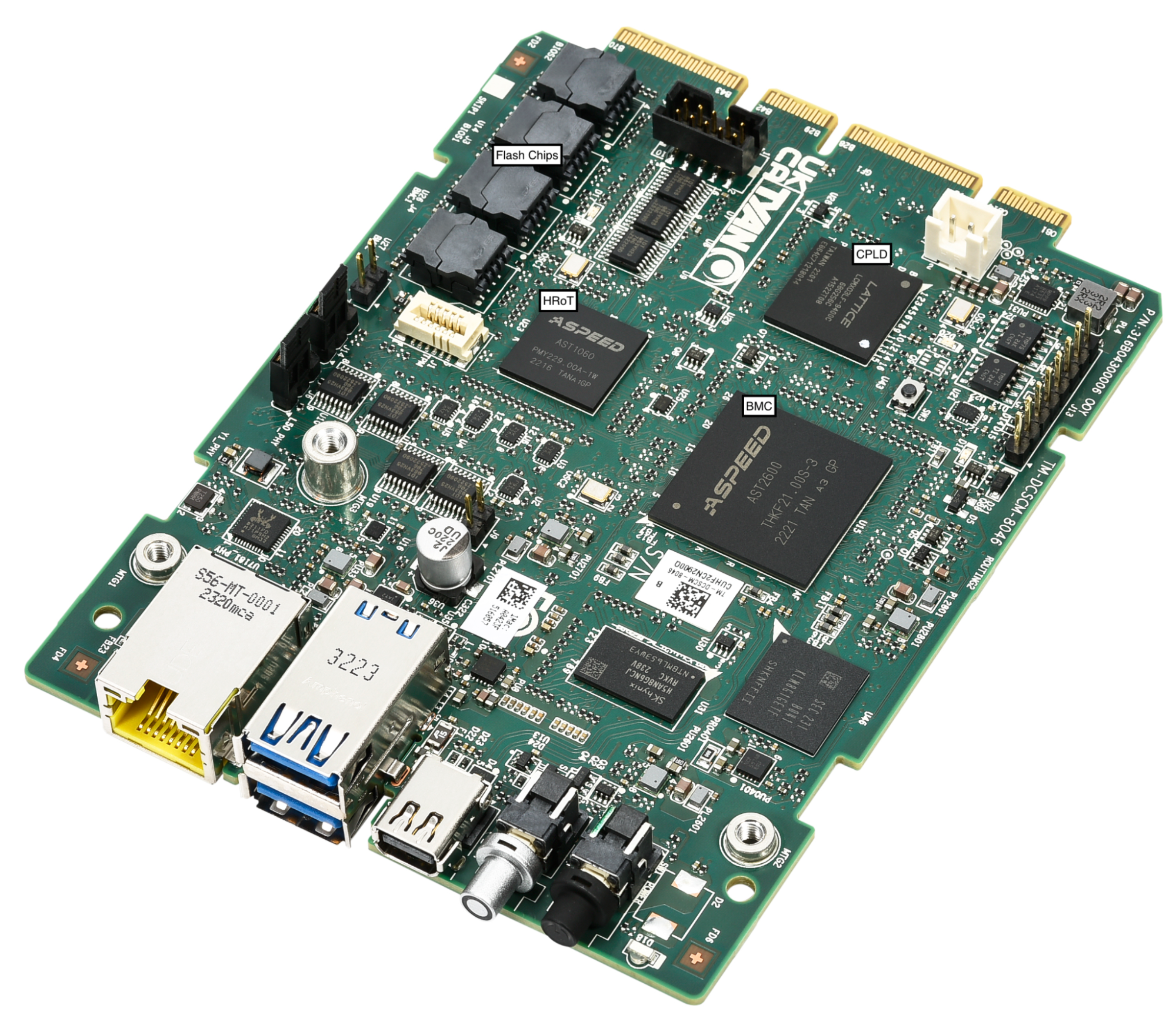
Additionally, we ensured that the critical components in the rear section of the system, such as the NIC and DC-SCM, were positioned away from the heatsink to promote the use of cooler available air within the system. Learning from past experience, the NIC temperature is monitored by the Baseboard Management Controller (BMC), which provides remote access to the server for administrative tasks and monitoring health metrics. Because the NIC has a built-in feature to protect itself from overheating by going into standby mode when the chip temperature reaches critical limits, it is important to provide air at the lowest possible temperature. As a reference, the temperature of the air right behind the CPU heatsink can reach 70°C or higher, whereas behind the memory banks, it would reach about 55°C under the same circumstances. The image below shows the internal placement of the most relevant components considered while building the thermal solution.
Using air as cold as possible to cool down any component will increase overall system reliability, preventing potential thermal issues and unplanned system shutdowns. That’s why our fan algorithm uses every thermal sensor available to ensure thermal health while using the minimum possible amount of energy.
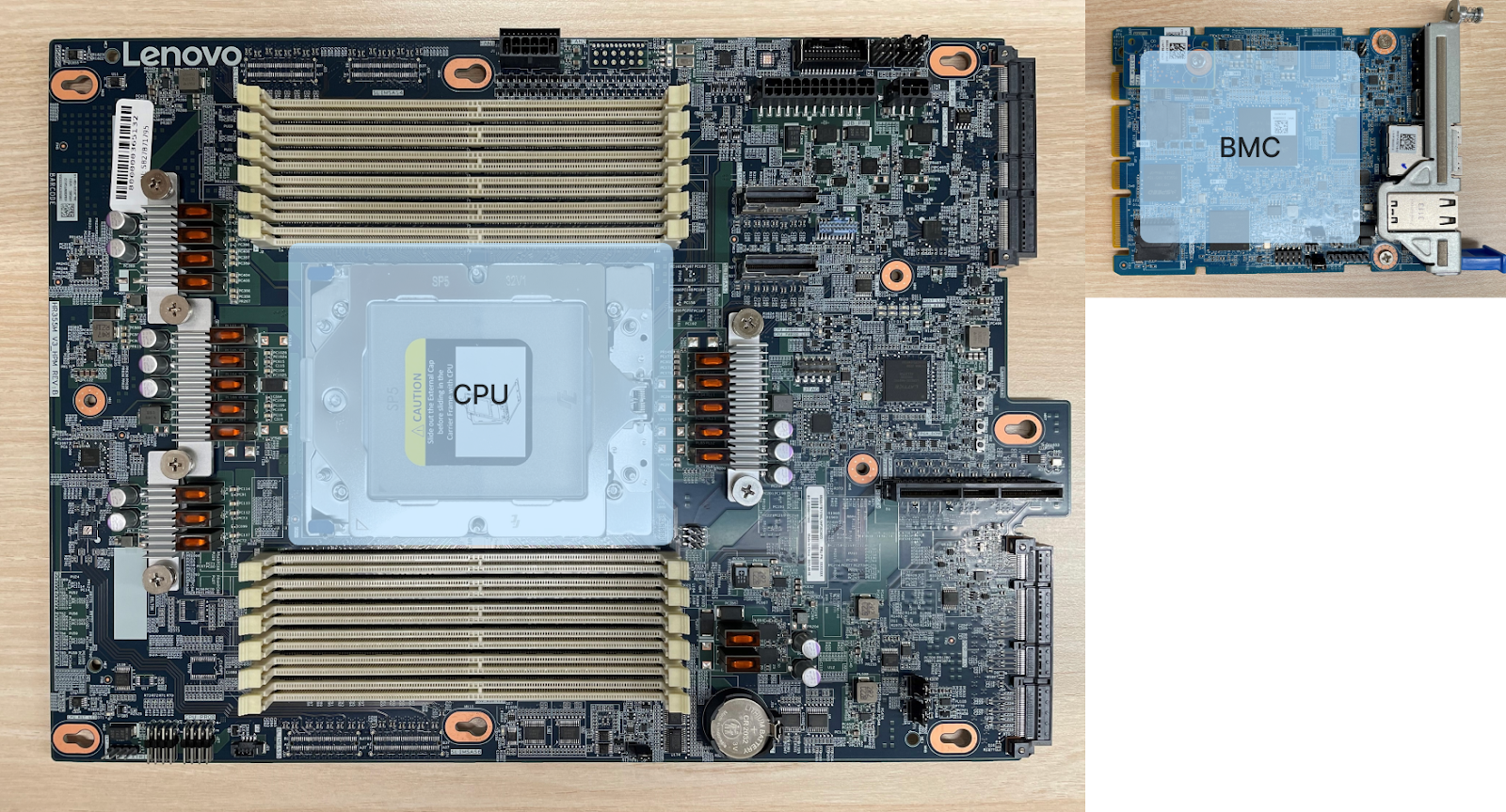
Components inside the compute server from one of our vendors, viewed from the rear of the server. (Illustration courtesy of vendor.)
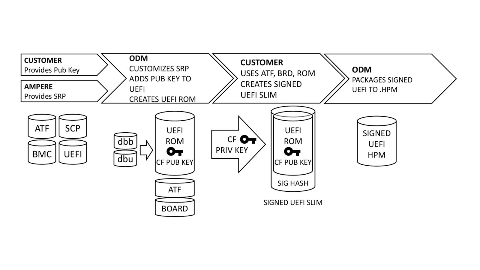
1️. Host Processor Module (HPM)
8. Power Distribution Board (PDB)
2️. DIMMs (x12)
9. GPUs (up to 2)
3️. CPU (under CPU heatsink)
10. GPU riser card
4. CPU heatsink
11. GPU riser cage
5. System fans (x4: 80mm, dual rotor)
12. Power Supply Units, PSUs (x2)
6. Bracket with power button and intrusion switch
13. DC-SCM 2.0 module
7. E1.S SSD
14. OCP 3.0 module
Making hardware flexible
With the same thought process of optimizing system layout, we decided to use a PCIe riser above the Power Supply Units (PSUs), enabling the support of up to 2x single wide GPU add-in cards. Once again, the combination of high-performing fans with strategic system architecture gave us the capability to add up to 400W to the original power envelope and incorporate accelerators used in our new and recently announced AI and ML features.
Hardware lead times are typically long, certainly when compared to software development. Therefore, a reliable strategy for hardware flexibility is imperative in this rapidly changing environment for specialized computing. When we started evaluating Gen 12 hardware architecture and early concept design, we didn’t know for sure we would be needing to implement GPUs for this generation, let alone how many or which type. However, highly efficient design and intentional due diligence analyzing hypothetical use cases help ensure flexibility and scalability of our thermal solution, supporting new requirements from our product teams, and ultimately providing the best solutions to our customers.
Rack-integrated solutions
We are also increasing the volume of integrated racks shipped to our global colocation facilities. Due to the expected increase in rack shipments, it is now more important that we also increase the corresponding mechanical and thermal test coverage from system level (L10) to rack level (L11).
Since our servers don’t use the full depth of a standard rack in order to leave room for cable management and Power Distribution Units (PDUs), there is another fluid mechanics factor that we need to consider to improve our holistic solution.
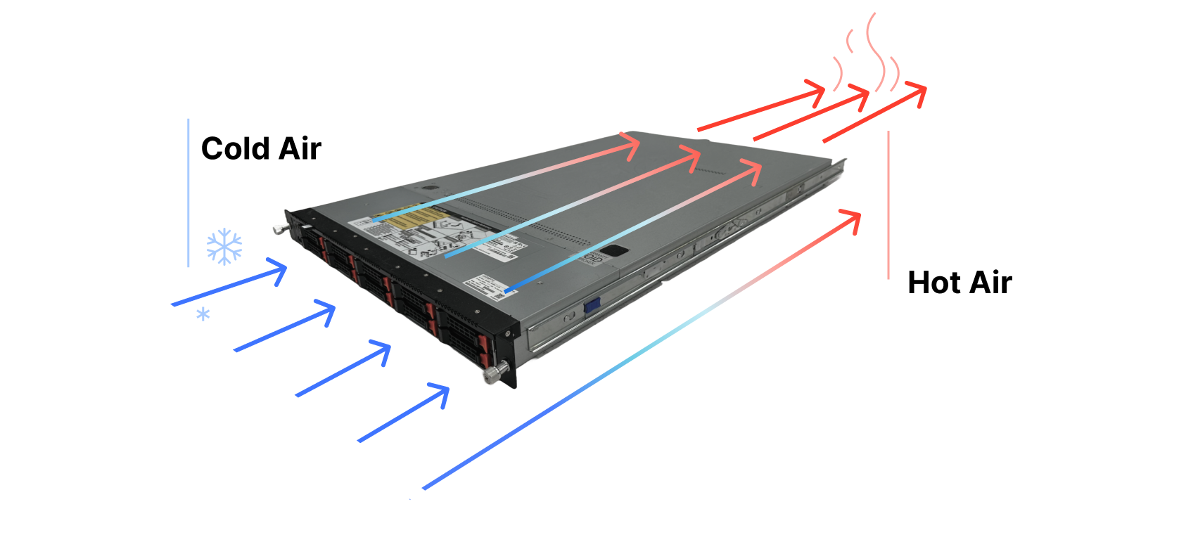
We design our hardware based on one of the most typical data center architectures, which have alternating cold and hot aisles. Fans at the front of the server pull in cold air from the corresponding aisle, the air then flows through the server, cooling down the internal components and the hot air is exhausted into the adjacent aisle, as illustrated in the diagram below.
A conventional air-flow diagram of a standard server where the cold air enters from the front of the server and hot air leaves through the rear side of the system.
In fluid dynamics, the minimum effort principle will drive fluids (air in this case) to move where there is less resistance — i.e. wherever it takes less energy to get from point A to point B. With the help of fans forcing air to flow inside the server and pushing it through the rear, the more crowded systems will naturally get less air than those with more space where the air can move around. Since we need more airflow to pass through the systems with higher power demands, we’ve also ensured that the rack configuration keeps these systems in the bottom of the rack where air tends to be at a lower temperature. Remember that heat rises, so even within the cold aisle, there can be a small but important temperature difference between the bottom and the top section of the rack. It is our duty as hardware engineers to use thermodynamics in our favor.
Conclusion
Our new generation of hardware is live in our data centers and it represents a significant leap forward in our efficiency, reliability, and sustainability commitments. Combining optimal heat sink design, thoughtful fan selection, and meticulous system layout and hardware architecture, we are confident that these new servers will operate smoothly in our global network with diverse environmental conditions, maintaining optimal performance of our Connectivity Cloud.
Come join us at Cloudflare to help deliver a better Internet!
Cloudflare is thrilled to announce the general deployment of our next generation of servers — Gen 12 powered by AMD EPYC 9684X (code name “Genoa-X”) processors. This next generation focuses on delivering exceptional performance across all Cloudflare services, enhanced support for AI/ML workloads, significant strides in power efficiency, and improved security features.
Here are some key performance indicators and feature improvements that this generation delivers as compared to the prior generation:
Beginning with performance, with close engineering collaboration between Cloudflare and AMD on optimization, Gen 12 servers can serve more than twice as many requests per second (RPS) as Gen 11 servers, resulting in lower Cloudflare infrastructure build-out costs.
Next, our power efficiency has improved significantly, by more than 60% in RPS per watt as compared to the prior generation. As Cloudflare continues to expand our infrastructure footprint, the improved efficiency helps reduce Cloudflare’s operational expenditure and carbon footprint as a percentage of our fleet size.
Third, in response to the growing demand for AI capabilities, we’ve updated the thermal-mechanical design of our Gen 12 server to support more powerful GPUs. This aligns with the Workers AI objective to support larger large language models and increase throughput for smaller models. This enhancement underscores our ongoing commitment to advancing AI inference capabilities
Fourth, to underscore our security-first position as a company, we’ve integrated hardware root of trust (HRoT) capabilities to ensure the integrity of boot firmware and board management controller firmware. Continuing to embrace open standards, the baseboard management and security controller (Data Center Secure Control Module or OCP DC-SCM) that we’ve designed into our systems is modular and vendor-agnostic, enabling a unified openBMC image, quicker prototyping, and allowing for reuse.
Finally, given the increasing importance of supply assurance and reliability in infrastructure deployments, our approach includes a robust multi-vendor strategy to mitigate supply chain risks, ensuring continuity and resiliency of our infrastructure deployment.
Cloudflare is dedicated to constantly improving our server fleet, empowering businesses worldwide with enhanced performance, efficiency, and security.
Gen 12 Servers
Let’s take a closer look at our Gen 12 server. The server is powered by a 4th generation AMD EPYC Processor, paired with 384 GB of DDR5 RAM, 16 TB of NVMe storage, a dual-port 25 GbE NIC, and two 800 watt power supply units.
During the design phase, we conducted an extensive survey of the CPU landscape. These options offer valuable choices as we consider how to shape the future of Cloudflare’s server technology to match the needs of our customers. We evaluated many candidates in the lab, and short-listed three standout CPU candidates from the 4th generation AMD EPYC Processor lineup: Genoa 9654, Bergamo 9754, and Genoa-X 9684X for production evaluation. The table below summarizes the differences in specifications of the short-listed candidates for Gen 12 servers against the AMD EPYC 7713 used in our Gen 11 servers. Notably, all three candidates offer significant increase in core count and marked increase in all core boost clock frequency.
*Note: AMD EPYC 7713 all core boost clock frequency of 2.7 GHz is not an official specification of the CPU but based on data collected at Cloudflare production fleet.
During production evaluation, the configuration of all three CPUs were optimized to the best of our knowledge, including thermal design power (TDP) configured to 400W for maximum performance. The servers are set up to run the same processes and services like any other server we have in production, which makes for a great side-by-side comparison.
Milan 7713
Genoa 9654
Bergamo 9754
Genoa-X 9684X
Production performance (request per second) multiplier
1x
2x
2.15x
2.45x
Production efficiency (request per second per watt) multiplier
1x
1.33x
1.38x
1.63x
AMD EPYC Genoa-X in Cloudflare Gen 12 server
Each of these CPUs outperforms the previous generation of processors by at least 2x. AMD EPYC 9684X Genoa-X with 3D V-cache technology gave us the greatest performance improvement, at 2.45x, when compared against our Gen 11 servers with AMD EPYC 7713 Milan.
Comparing the performance between Genoa-X 9684X and Genoa 9654, we see a ~22.5% performance delta. The primary difference between the two CPUs is the amount of L3 cache available on the CPU. Genoa-X 9684X has 1152 MB of L3 cache, which is three times the Genoa 9654 with 384 MB of L3 cache. Cloudflare workloads benefit from more low level cache being accessible and avoid the much larger latency penalty associated with fetching data from memory.
Genoa-X 9684X CPU delivered ~22.5% improved performance consuming the same amount of 400W power compared to Genoa 9654. The 3x larger L3 cache does consume additional power, but only at the expense of sacrificing 3% of highest achievable all core boost frequency on Genoa-X 9684X, a favorable trade-off for Cloudflare workloads.
More importantly, Genoa-X 9684X CPU delivered 145% performance improvement with only 50% system power increase, offering a 63% power efficiency improvement that will help drive down operational expenditure tremendously. It is important to note that even though a big portion of the power efficiency is due to the CPU, it needs to be paired with optimal thermal-mechanical design to realize the full benefit. Earlier last year, we made the thermal-mechanical design choice to double the height of the server chassis to optimize rack density and cooling efficiency across our global data centers. We estimated that moving from 1U to 2U would reduce fan power by 150W, which would decrease system power from 750 watts to 600 watts. Guess what? We were right — a Gen 12 server consumes 600 watts per system at a typical ambient temperature of 25°C.
While high performance often comes at a higher price, fortunately AMD EPYC 9684X offer an excellent balance between cost and capability. A server designed with this CPU provides top-tier performance without necessitating a huge financial outlay, resulting in a good Total Cost of Ownership improvement for Cloudflare.
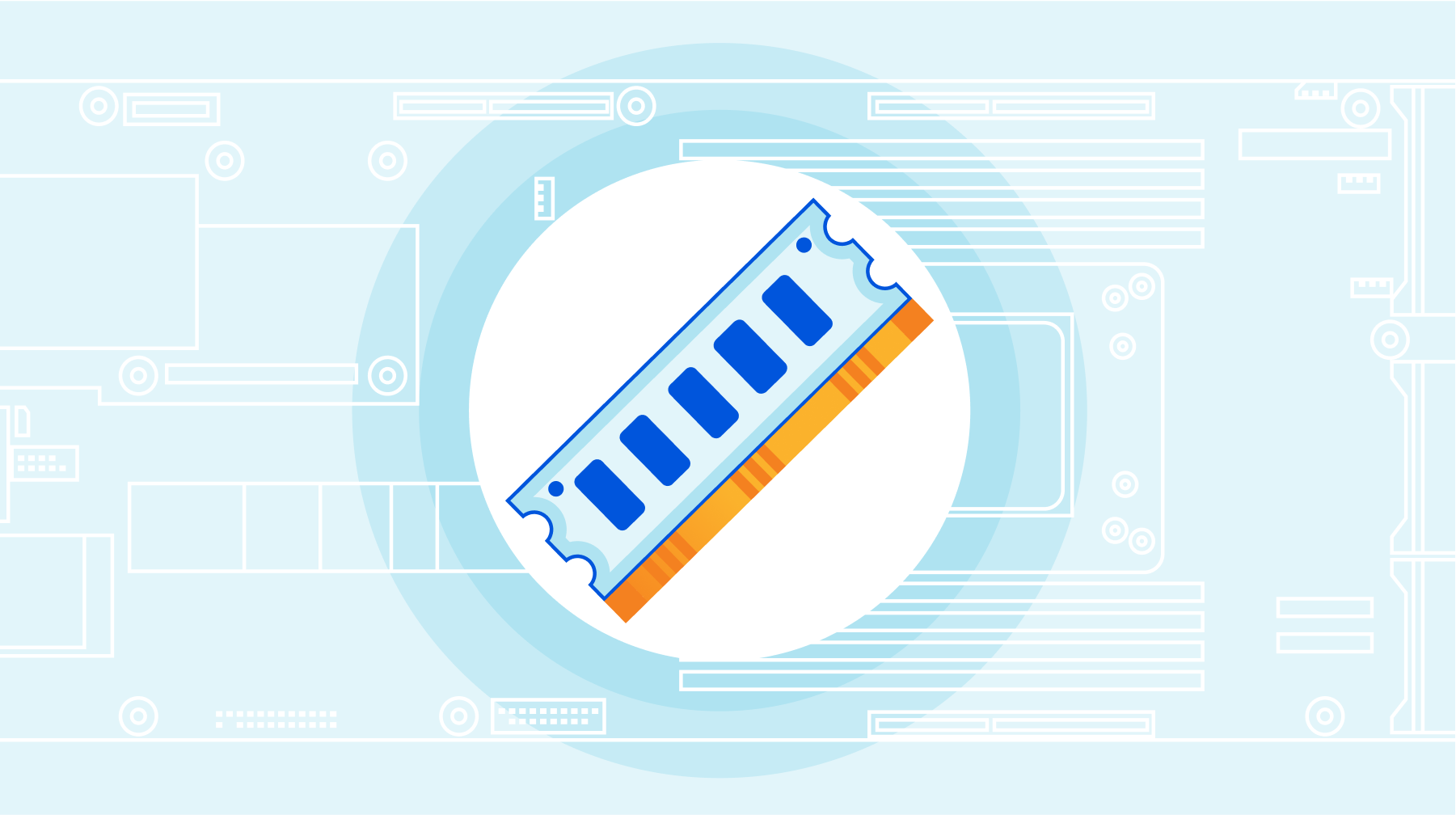
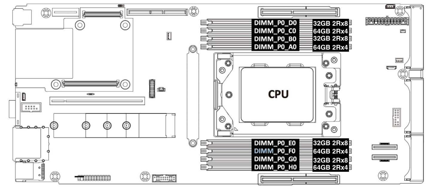
Memory
AMD Genoa-X CPU supports twelve memory channels of DDR5 RAM up to 4800 mega transfers per second (MT/s) and per socket Memory Bandwidth of 460.8 GB/s. The twelve channels are fully utilized with 32 GB ECC 2Rx8 DDR5 RDIMM with one DIMM per channel configuration for a combined total memory capacity of 384 GB.
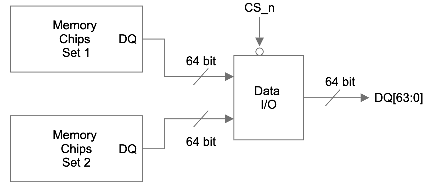
Choosing the optimal memory capacity is a balancing act, as maintaining an optimal memory-to-core ratio is important to make sure CPU capacity or memory capacity is not wasted. Some may remember that our Gen 11 servers with 64 core AMD EPYC 7713 CPUs are also configured with 384 GB of memory, which is about 6 GB per core. So why did we choose to configure our Gen 12 servers with 384 GB of memory when the core count is growing to 96 cores? Great question! A lot of memory optimization work has happened since we introduced Gen 11, including some that we blogged about, like Bot Management code optimization and our transition to highly efficient Pingora. In addition, each service has a memory allocation that is sized for optimal performance. The per-service memory allocation is programmed and monitored utilizing Linux control group resource management features. When sizing memory capacity for Gen 12, we consulted with the team who monitor resource allocation and surveyed memory utilization metrics collected from our fleet. The result of the analysis is that the optimal memory-to-core ratio is 4 GB per CPU core, or 384 GB total memory capacity. This configuration is validated in production. We chose dual rank memory modules over single rank memory modules because they have higher memory throughput, which improves server performance (read more about memory module organization and its effect on memory bandwidth).
The table below shows the result of running the Intel Memory Latency Checker (MLC) tool to measure peak memory bandwidth for the system and to compare memory throughput between 12 channels of dual-rank (2Rx8) 32 GB DIMM and 12 channels of single rank (1Rx4) 32 GB DIMM. Dual rank DIMMs have slightly higher (1.8%) read memory bandwidth, but noticeably higher write bandwidth. As write ratios increased from 25% to 50%, the memory throughput delta increased by 10%.
Benchmark
Dual rank advantage over single rank
Intel MLC ALL Reads
101.8%
Intel MLC 3:1 Reads-Writes
107.7%
Intel MLC 2:1 Reads-Writes
112.9%
Intel MLC 1:1 Reads-Writes
117.8%
Intel MLC Stream-triad like
108.6%
The table below shows the result of running the AMD STREAM benchmark to measure sustainable main memory bandwidth in MB/s and the corresponding computation rate for simple vector kernels. In all 4 types of vector kernels, dual rank DIMMs provide a noticeable advantage over single rank DIMMs.
Benchmark
Dual rank advantage over single rank
Stream Copy
115.44%
Stream Scale
111.22%
Stream Add
109.06%
Stream Triad
107.70%
Storage
Cloudflare’s Gen X server and Gen 11 server support M.2 form factor drives. We liked the M.2 form factor mainly because it was compact. The M.2 specification was introduced in 2012, but today, the connector system is dated and the industry has concerns about its ability to maintain signal integrity with the high speed signal specified by PCIe 5.0 and PCIe 6.0 specifications. The 8.25W thermal limit of the M.2 form factor also limits the number of flash dies that can be fitted, which limits the maximum supported capacity per drive. To address these concerns, the industry has introduced the E1.S specification and is transitioning from the M.2 form factor to the E1.S form factor.
In Gen 12, we are making the change to the EDSFF E1 form factor, more specifically the E1.S 15mm. E1.S 15mm, though still in a compact form factor, provides more space to fit more flash dies for larger capacity support. The form factor also has better cooling design to support more than 25W of sustained power.
While the AMD Genoa-X CPU supports 128 PCIe 5.0 lanes, we continue to use NVMe devices with PCIe Gen 4.0 x4 lanes, as PCIe Gen 4.0 throughput is sufficient to meet drive bandwidth requirements and keep server design costs optimal. The server is equipped with two 8 TB NVMe drives for a total of 16 TB available storage. We opted for two 8 TB drives instead of four 4 TB drives because the dual 8 TB configuration already provides sufficient I/O bandwidth for all Cloudflare workloads that run on each server.
Sequential Read (MB/s) :
6,700
Sequential Write (MB/s) :
4,000
Random Read IOPS:
1,000,000
Random Write IOPS:
200,000
Endurance
1 DWPD
PCIe GEN4 x4 lane throughput
7880 MB/s
Storage devices performance specification
Network
Cloudflare servers and top-of-rack (ToR) network equipment operate at 25 GbE speeds. In Gen 12, we utilized a DC-MHS motherboard-inspired design, and upgraded from an OCP 2.0 form factor to an OCP 3.0 form factor, which provides tool-less serviceability of the NIC. The OCP 3.0 form factor also occupies less space in the 2U server compared to PCIe-attached NICs, which improves airflow and frees up space for other application-specific PCIe cards, such as GPUs.
Cloudflare has been using the Mellanox CX4-Lx EN dual port 25 GbE NIC since our Gen 9 servers in 2018. Even though the NIC has served us well over the years, we are single sourced. During the pandemic, we were faced with supply constraints and extremely long lead times. The team scrambled to qualify the Broadcom M225P dual port 25 GbE NIC as our second-sourced NIC in 2022, ensuring we could continue to turn up servers to serve customer demand. With the lessons learned from single-sourcing the Gen 11 NIC, we are now dual-sourcing and have chosen the Intel Ethernet Network Adapter E810 and NVIDIA Mellanox ConnectX-6 Lx to support Gen 12. These two NICs are compliant with the OCP 3.0 specification and offer more MSI-X queues that can then be mapped to the increased core count on the AMD EPYC 9684X. The Intel Ethernet Network Adapter comes with an additional advantage, offering full Generic Segmentation Offload (GSO) support including VLAN-tagged encapsulated traffic, whereast many vendors either only support Partial GSO or do not support it at all today. With Full GSO support, the kernel spent noticeably less time in softirq segmenting packets, and servers with Intel E810 NICs are processing approximately 2% more requests per second.
Improved security with DC-SCM: Project Argus
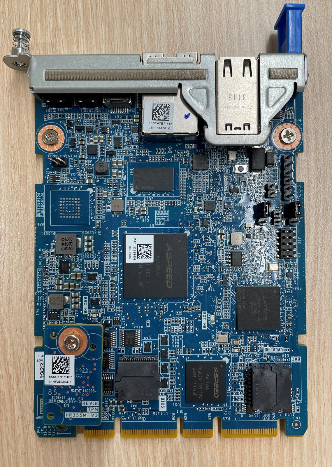
DC-SCM in Gen 12 server (Project Argus)
Gen 12 servers are integrated with Project Argus, one of the industry first implementations of Data Center Secure Control Module 2.0 (DC-SCM 2.0). DC-SCM 2.0 decouples server management and security functions away from the motherboard. The baseboard management controller (BMC), hardware root of trust (HRoT), trusted platform module (TPM), and dual BMC/BIOS flash chips are all installed on the DC-SCM.
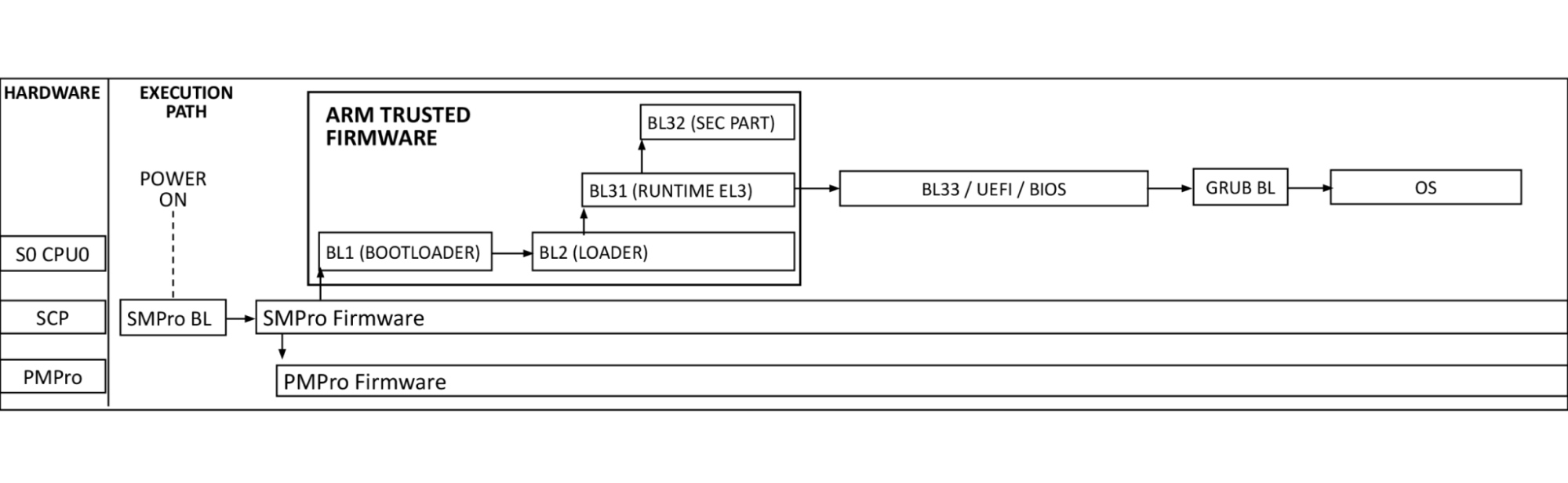
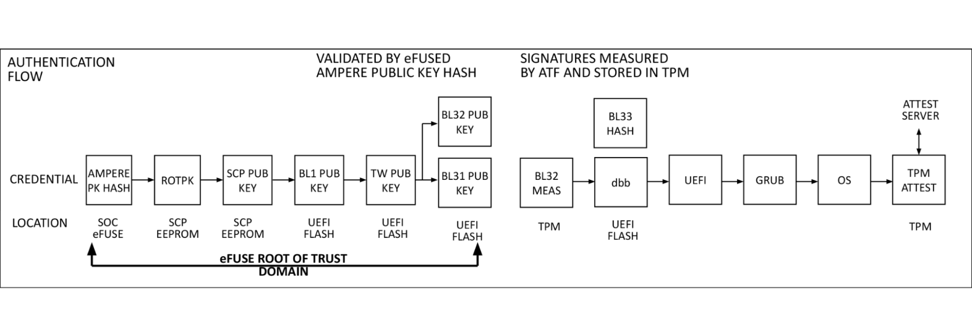
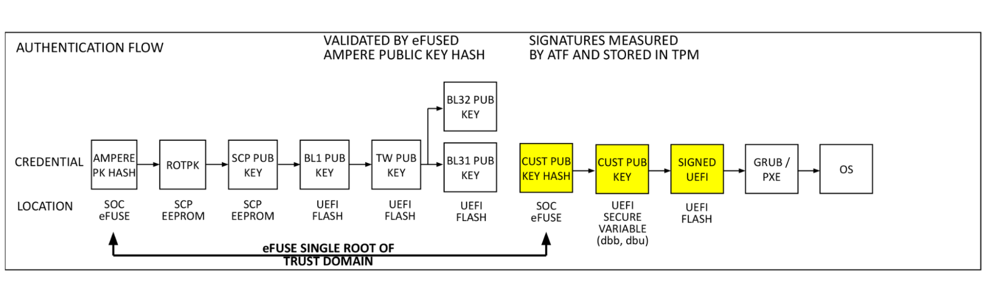
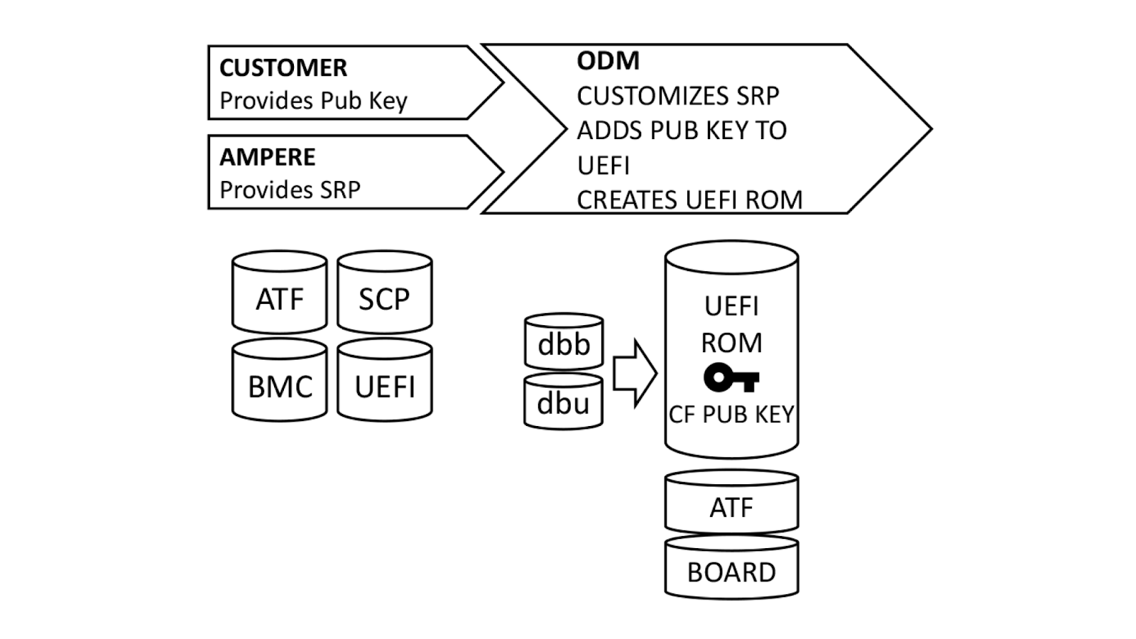
On our Gen X and Gen 11 server, Cloudflare moved our secure boot trust anchor from the system Basic Input/Output System (BIOS) or the Unified Extensible Firmware Interface (UEFI) firmware to hardware-rooted boot integrity — AMD’s implementation of Platform Secure Boot (PSB) or Ampere’s implementation of Single Domain Secure Boot. These solutions helped secure Cloudflare infrastructure from BIOS / UEFI firmware attacks. However, we are still vulnerable to out-of-band attacks through compromising the BMC firmware. BMC is a microcontroller that provides out-of-band monitoring and management capabilities for the system. When compromised, attackers can read processor console logs accessible by BMC and control server power states for example. On Gen 12, the HRoT on the DC-SCM serves as the trust store of cryptographic keys and is responsible to authenticate the BIOS/UEFI firmware (independent of CPU vendor) and the BMC firmware for secure boot process.
In addition, on the DC-SCM, there are additional flash storage devices to enable storing back-up BIOS/UEFI firmware and BMC firmware to allow rapid recovery when a corrupted or malicious firmware is programmed, and to be resilient to flash chip failure due to aging.
These updates make our Gen 12 server more secure and more resilient to firmware attacks.
Power
A Gen 12 server consumes 600 watts at a typical ambient temperature of 25°C. Even though this is a 50% increase from the 400 watts consumed by the Gen 11 server, as mentioned above in the CPU section, this is a relatively small price to pay for a 145% increase in performance. We’ve paired the server up with dual 800W common redundant power supplies (CRPS) with 80 PLUS Titanium grade efficiency. Both power supply units (PSU) operate actively with distributed power and current. The units are hot-pluggable, allowing the server to operate with redundancy and maximize uptime.
80 PLUS is a PSU efficiency certification program. The Titanium grade efficiency PSU is 2% more efficient than the Platinum grade efficiency PSU between typical operating load of 25% to 50%. 2% may not sound like a lot, but considering the size of Cloudflare fleet with servers deployed worldwide, 2% savings over the lifetime of all Gen 12 deployment is a reduction of more than 7 GWh, equivalent to carbon sequestered by more than 3400 acres of U.S. forests in one year. This upgrade also means our Gen 12 server complies with EU Lot9 requirements and can be deployed in the EU region.
80 PLUS certification
10%
20%
50%
100%
80 PLUS Platinum
–
92%
94%
90%
80 PLUS Titanium
90%
94%
96%
91%
Drop-in GPU support
Demand for machine learning and AI workloads exploded in 2023, and Cloudflare introduced Workers AI to serve the needs of our customers. Cloudflare retrofitted or deployed GPUs worldwide in a portion of our Gen 11 server fleet to support the growth of Workers AI. Our Gen 12 server is also designed to accommodate the addition of more powerful GPUs. This gives Cloudflare the flexibility to support Workers AI in all regions of the world, and to strategically place GPUs in regions to reduce inference latency for our customers. With this design, the server can run Cloudflare’s full software stack. During times when GPUs see lower utilization, the server continues to serve general web requests and remains productive.
The electrical design of the motherboard is designed to support up to two PCIe add-in cards and the power distribution board is sized to support an additional 400W of power. The mechanics are sized to support either a single FHFL (full height, full length) double width GPU PCIe card, or two FHFL single width GPU PCIe cards. The thermal solution including the component placement, fans, and air duct design are sized to support adding GPUs with TDP up to 400W.
Looking to the future
Gen 12 Servers are currently deployed and live in multiple Cloudflare data centers worldwide, and already process millions of requests per second. Cloudflare’s EPYC journey has not ended — the 5th-gen AMD EPYC CPUs (code name “Turin”) are already available for testing, and we are very excited to start the architecture planning and design discussion for the Gen 13 server. Come join us at Cloudflare to help build a better Internet!
In 2023, Cloudflare introduced a new load balancing solution supporting Local Traffic Management (LTM). This year, we took it a step further by introducing support for layer 4 load balancing to private networks via Spectrum. Now, organizations can seamlessly balance public HTTP(S), TCP, and UDP traffic to their privately hosted applications. Today, we’re thrilled to unveil our latest enhancement: support for end-to-end private traffic flows as well as WARP authenticated device traffic, eliminating the need for dedicated hardware load balancers! These groundbreaking features are powered by the enhanced integration of Cloudflare load balancing with our Cloudflare One platform, and are available to our enterprise customers. With this upgrade, our customers can now utilize Cloudflare load balancers for both public and private traffic directed at private networks.
Cloudflare Load Balancing today
Before discussing the new features, let’s review Cloudflare’s existing load balancing support and the challenges customers face.
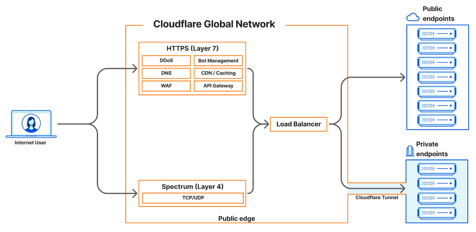
Cloudflare currently supports four main load balancing traffic flows:
Internet-facing load balancers connecting to publicly accessible endpoints at layer 7, supporting HTTP(S).
Internet-facing load balancers connecting to publicly accessible endpoints at layer 4 (Spectrum), supporting TCP and UDP services
Internet-facing load balancers connecting to private endpoints at layer 7 HTTP(S) via Cloudflare Tunnels.
Internet-facing load balancers connecting to private endpoints at layer 4 (Spectrum), supporting TCP and UDP services via Cloudflare Tunnels.
One of the biggest advantages of Cloudflare’s load balancing solutions is the elimination of hardware costs and maintenance. Unlike hardware-based load balancers, which are costly to purchase, license, operate, and upgrade, Cloudflare’s solution requires no hardware. There’s no need to buy additional modules or new licenses, and you won’t face end-of-life issues with equipment that necessitate costly replacements.
With Cloudflare, you can focus on innovation and growth. Load balancers are deployed in every Cloudflare data center across the globe, in over 300 cities, providing virtually unlimited scale and capacity. You never need to worry about bandwidth constraints, deployment locations, extra hardware modules, downtime, upgrades, or supply chain constraints. Cloudflare’s global Anycast network ensures that every customer connects to a nearby data center and load balancer, where policies, rules, and steering are applied efficiently. And now, the resilience, scale, and simplicity of Cloudflare load balancers can be integrated into your private networks! We have worked hard to ensure that Cloudflare load balancers are highly available and disaster ready, from the core to the edge – even when datacenters lose power.
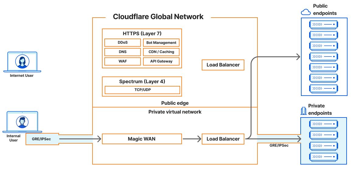
Keeping private resources private with Magic WAN
Before today’s announcement, all of Cloudflare’s load balancers operating at layer 4 have been connected to the public Internet. Customers have been able to secure the traffic flowing to their load balancers with WAF rules and Zero Trust policies, but some customers would prefer to keep certain resources private and under no circumstances exposed to the Internet. It’s been possible to isolate origin servers and endpoints this way, which can exist on private networks that are only accessible via Cloudflare Tunnels. And as of today, we can offer a similar level of isolation to customers’ layer 4 load balancers.
In our previous LTM blog post, we discussed connecting these internal or private resources to the Cloudflare global network and how Cloudflare would soon introduce load balancers that are accessible via private IP addresses. Unlike other Cloudflare load balancers, these do not have an associated hostname. Rather, they are accessible via an RFC 1918 private IP address. In the land of load balancers, this is often referred to as a virtual IP (VIP). As of today, load balancers that are accessible at private IPs can now be used within a virtual network to isolate traffic to a certain set of Cloudflare tunnels, enabling customers to load balance traffic within their private network without exposing applications to the public Internet.
The question you might be asking is, “If I have a private IP load balancer and privately hosted applications, how do I or my users actually reach these now-private services?”
Cloudflare Magic WAN can now be used as an on-ramp in tandem with Cloudflare load balancers that are accessible via an assigned private IP address. Magic WAN provides a secure and high-performance connection to internal resources, ensuring that traffic remains private and optimized across our global network. With Magic WAN, customers can connect their corporate networks directly to Cloudflare’s global network with GRE or IPSec tunnels, maintaining privacy and security while enjoying seamless connectivity. The Magic WAN Connector easily establishes connectivity to Cloudflare without the need to configure network gear, and it can be deployed at any physical or cloud location! With the enhancements to Cloudflare’s load balancing solution, customers can confidently keep their corporate applications resilient while maintaining the end-to-end privacy and security of their resources.
This enhancement opens up numerous use cases for internal load balancing, such as managing traffic between different data centers, efficiently routing traffic for internally hosted applications, optimizing resource allocation for critical applications, and ensuring high availability for internal services. Organizations can now replace traditional hardware-based load balancers, reducing complexity and lowering costs associated with maintaining physical infrastructure. By leveraging Cloudflare load balancing and Magic WAN, companies can achieve greater flexibility and scalability, adapting quickly to changing network demands without the need for additional hardware investments.
But what about latency? Load balancing is all about keeping your applications resilient and performant and Cloudflare was built with speed at its core. There is a Cloudflare datacenter within 50ms of 95% of the Internet-connected population globally! Now, we support all Cloudflare One on-ramps to not only provide seamless and secure connectivity, but also to dramatically reduce latency compared to legacy solutions. Load balancing also works seamlessly with Argo Smart Routing to intelligently route around network congestion to improve your application performance by up to 30%! Check out the blogs here and here to read more about how Cloudflare One can reduce application latency.
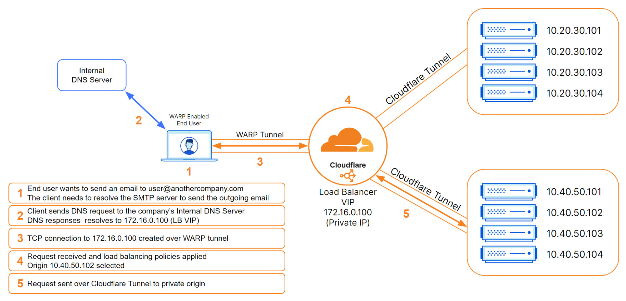
Supporting distributed users with Cloudflare WARP
But what about when users are distributed and not connected to the local corporate network? Cloudflare WARP can now be used as an on-ramp to reach Cloudflare load balancers that are configured with private IP addresses. The Cloudflare WARP client allows you to protect corporate devices by securely and privately sending traffic from those devices to Cloudflare’s global network, where Cloudflare Gateway can apply advanced web filtering. The WARP client also makes it possible to apply advanced Zero Trust policies that check a device’s health before it connects to corporate applications.
In this load balancing use case, WARP pairs up perfectly with Cloudflare Tunnels so that customers can place their private origins within virtual networks to help either isolate traffic or handle overlapping private IP addresses. Once these virtual networks are defined, administrators can configure WARP profiles to allow their users to connect to the proper virtual networks. Once connected, WARP takes the configuration of the virtual networks and installs routes on the end users’ devices. These routes will tell the end user’s device how to reach the Cloudflare load balancer that was created with a private, non-publicly routable IP address. The administrator could then create a DNS record locally that would point to that private IP address. Once DNS resolves locally, the device would route all subsequent traffic over the WARP connection. This is all seamless to the user and occurs with minimal latency.
How we connected load balancing to Cloudflare One
In contrast to public L4 or L7 load balancers, private L4 load balancers are not going to have publicly addressable hostnames or IP addresses, but we still need to be able to handle their traffic. To make this possible, we had to integrate existing load balancing services with private networking services created by our Cloudflare One team. To do this, upon creation of a private load balancer, we now assign a private IP address within the customer’s virtual network. When traffic destined for a private load balancer enters Cloudflare, our private networking services make a request to load balancing to determine which endpoint to connect to. The information in the response from load balancing is used to connect directly to a privately hosted endpoint via a variety of secure traffic off-ramps. This differs significantly from our public load balancers where traffic is off-ramped to the public internet. In fact, we can now direct traffic from any on-ramp to any off-ramp! This allows for significant flexibility in architecture. For example, not only can we direct WARP traffic to an endpoint connected via GRE or IPSec, but we can also off-ramp this traffic to Cloudflare Tunnel, a CNI connection, or out to the public internet! Now, instead of purchasing a bespoke load balancing solution for each traffic type, like an application or network load balancer, you can configure a single load balancing solution to handle virtually any permutation of traffic that your business needs to run!
Getting started with internal load balancing
We are excited to be releasing these new load balancing features that solve critical connectivity issues for our customers and effectively eliminate the need for a hardware load balancer. Cloudflare load balancers now support end-to-end private traffic flows with Cloudflare One. To get started with configuring this feature, take a look at our load balancing documentation.
We are just getting started with our local traffic management load balancing support. There is so much more to come including user experience changes, enhanced layer 4 session affinity, new steering methods, refined control of egress ports, and more.
The threat resides in the chips’ data memory-dependent prefetcher, a hardware optimization that predicts the memory addresses of data that running code is likely to access in the near future. By loading the contents into the CPU cache before it’s actually needed, the DMP, as the feature is abbreviated, reduces latency between the main memory and the CPU, a common bottleneck in modern computing. DMPs are a relatively new phenomenon found only in M-series chips and Intel’s 13th-generation Raptor Lake microarchitecture, although older forms of prefetchers have been common for years.
[…]
The breakthrough of the new research is that it exposes a previously overlooked behavior of DMPs in Apple silicon: Sometimes they confuse memory content, such as key material, with the pointer value that is used to load other data. As a result, the DMP often reads the data and attempts to treat it as an address to perform memory access. This “dereferencing” of “pointers”—meaning the reading of data and leaking it through a side channel—is a flagrant violation of the constant-time paradigm.
[…]
The attack, which the researchers have named GoFetch, uses an application that doesn’t require root access, only the same user privileges needed by most third-party applications installed on a macOS system. M-series chips are divided into what are known as clusters. The M1, for example, has two clusters: one containing four efficiency cores and the other four performance cores. As long as the GoFetch app and the targeted cryptography app are running on the same performance cluster—even when on separate cores within that cluster—GoFetch can mine enough secrets to leak a secret key.
The attack works against both classical encryption algorithms and a newer generation of encryption that has been hardened to withstand anticipated attacks from quantum computers. The GoFetch app requires less than an hour to extract a 2048-bit RSA key and a little over two hours to extract a 2048-bit Diffie-Hellman key. The attack takes 54 minutes to extract the material required to assemble a Kyber-512 key and about 10 hours for a Dilithium-2 key, not counting offline time needed to process the raw data.
The GoFetch app connects to the targeted app and feeds it inputs that it signs or decrypts. As its doing this, it extracts the app secret key that it uses to perform these cryptographic operations. This mechanism means the targeted app need not perform any cryptographic operations on its own during the collection period.
Note that exploiting the vulnerability requires running a malicious app on the target computer. So it could be worse. On the other hand, like many of these hardware side-channel attacks, it’s not possible to patch.
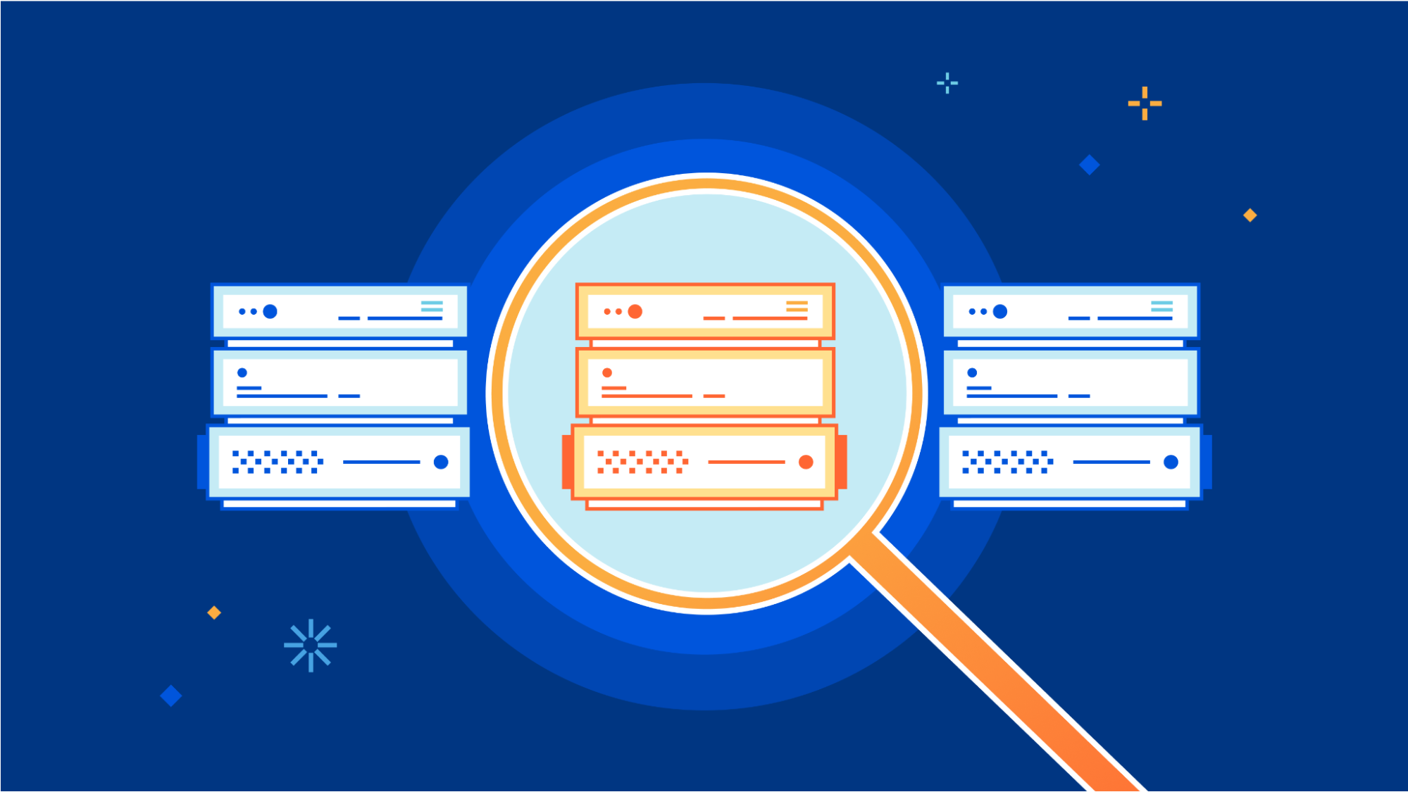
Cloudflare’s global network spans more than 310 cities in over 120 countries. That means thousands of servers geographically spread across different data centers, running services that protect and accelerate our customer’s Internet applications. Operating hardware at such a scale means that hardware can break anywhere and at any time. In such cases, our systems are engineered such that these failures cause little to no impact. However, detecting and managing server failure at scale requires automation. This blog aims to provide insights into the difficulties involved in handling broken servers and how we were able to simplify the process through automation.
Challenges dealing with broken servers
When a server is found to have faulty hardware and needs to be removed from production, it is considered broken and its state is set to Repair in the internal database where server status is tracked. In the past, our Data Center Operations team were essentially left to troubleshoot and diagnose broken servers on their own. They had to go through laborious tasks like performing queries to locate and repair servers, conducting diagnostics, reviewing results, evaluating if a server can be restored to production, and creating the necessary tickets for re-enabling servers and executing operations to put them back in production. Such effort can take hours for a single server alone, and can easily consume an engineer’s entire day.
As you can see, addressing server repairs was a labor-intensive process performed manually, Additionally, a lot of these servers remained powered on within the racks, wasting energy. With our fleet expanding rapidly, the attention of Data Center Operations is primarily devoted to supporting this growth, leaving less time to handle servers in need of repair.
It was clear that our infrastructure was growing too fast for us to be able to handle repairs and recovery, so we had to find a better way to handle these sorts of inefficiencies in our operations. This would allow our engineers to focus on the growth of our footprint while not abandoning repair and recovery – after all, these are still huge CapEx investments and wasted capacity that otherwise would have been fully utilized.
Using automation as an autonomous system
As members of the Infrastructure Software Systems and Automation team at Cloudflare, we primarily work on building tools and automation that help reduce excess work in order to ease the pressure on our operations teams, increase productivity, and enable people to execute operations with the highest efficiency.
Our team continuously strives to challenge our existing processes and systems, finding ways we can evolve them and make significant improvements – one of which is to build not just a typical automated system but an autonomous one. Building autonomous automations means creating systems that can operate independently, without the need for constant human intervention or oversight – a perfect example of this is Phoenix.
Introducing Phoenix
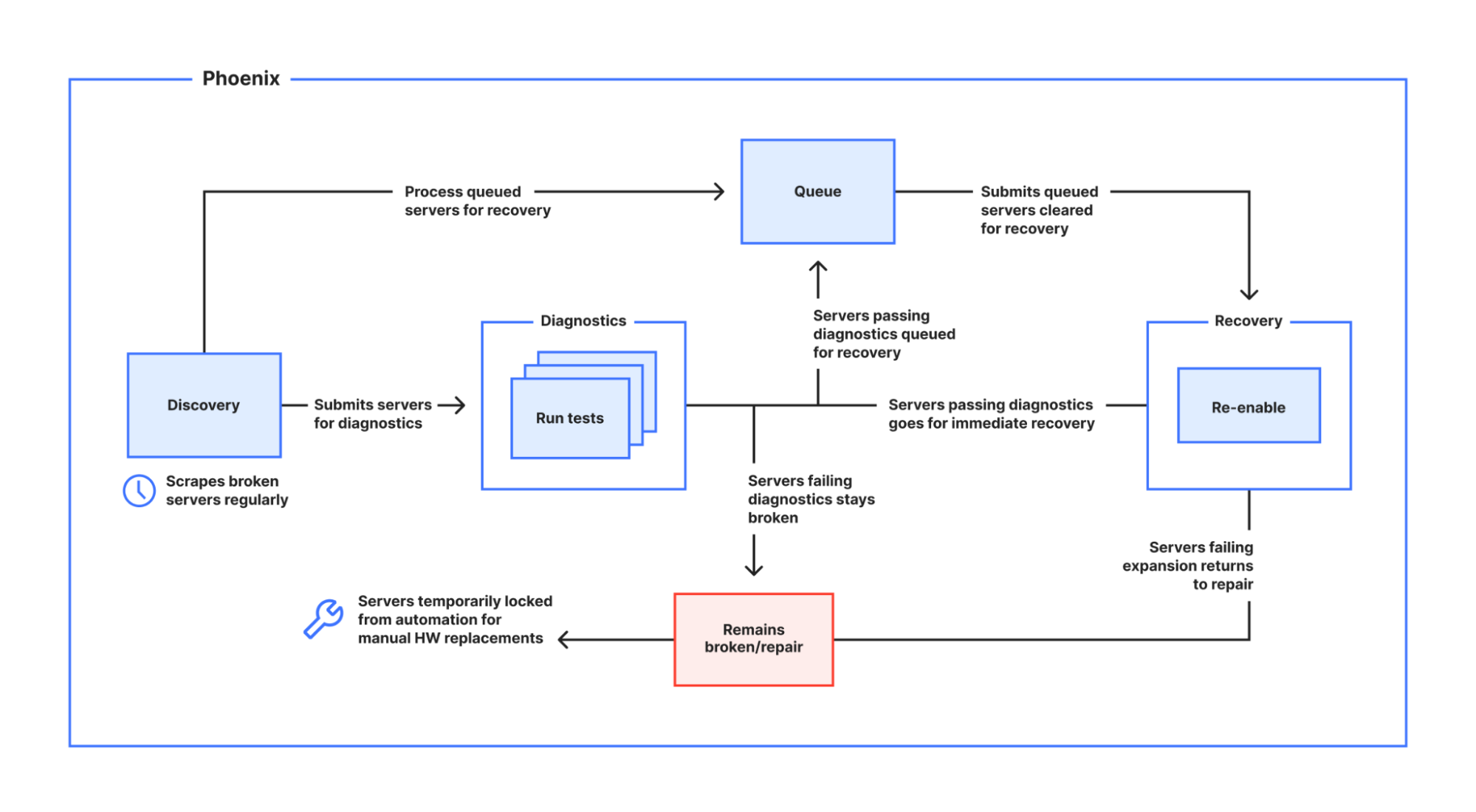
Phoenix is an autonomous diagnostics and recovery automation that runs at regular intervals to discover Cloudflare data centers with servers that are broken, performing diagnostics on detection, recovering those that pass diagnostics by re-provisioning, and ultimately re-enabling those that have successfully been re-provisioned in the safest and most unobtrusive way possible – all without requiring any human intervention! Should a server fail at any point in the process, Phoenix will take care of updating relevant tickets, even pinpointing the cause of the failure, and reverting the state of the server accordingly when needed – again, all without any human intervention!
The image below illustrates the whole process:
To better understand exactly how Phoenix works, let’s dive into some details about its core functionality.
Discovery
Discovery runs at a regular interval of 30 minutes, selecting a maximum of two Cloudflare data centers that have broken or repair state servers in its fleet, which are all configurable depending on business and operational needs, against which it can immediately execute diagnostics. At this rate, Phoenix is able to discover and operate on all broken servers in the fleet in about 3 days. On each run, it also detects data centers that may have broken servers already queued for recovery, and takes care of ensuring that the Recovery phase is executed immediately.
Diagnostics
Diagnostics takes care of running various tests across the broken servers of a selected data center in a single run, verifying viability of the hardware components, and identifying the candidates for recovery.
A diagnostic operation includes running the following:
Out-of-Band connectivity check This check determines the reachability of a device via out-of-band network. We employ IPMI (Intelligent Platform Management Interface) to ensure proper physical connectivity and accessibility of devices. This allows for effective monitoring and management of hardware components, enhancing overall system reliability and performance. Only devices that pass this check can progress to the Node Acceptance Testing phase.
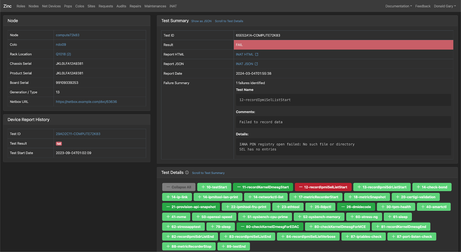
Node Acceptance Tests We leverage an existing internally-built tool called INAT (Integrated Node Acceptance Testing) that runs various tests suites/cases (Hardware Validation, Performance, etc.).
For every server that needs to be diagnosed, Phoenix will send relevant system instructions to have it boot into a custom Linux boot image, internally called INAT-image. Built into this image are the various tests that need to run when the server boots up, publishing the results to an internal resource in both human-readable (HTML) and machine-readable (JSON) formats, with the latter consumed and interpreted by Phoenix. Upon completion of the boot diagnostics, the server is powered off again to ensure it is not wasting energy.
Our node acceptance tests encompass a range of evaluations, including but not limited to benchmark testing, CPU/Memory/Storage checks, drive wiping, and various other assessments. Look out for an upcoming in-depth blog post covering INAT.
A summarized diagnostics result is immediately added to the tracking ticket, including pinpointing the exact cause of a failure.
Recovery
Recovery executes what we call an expansion operation, which in its first phase will provision the servers that pass diagnostics. The second phase is to re-enable the successfully provisioned servers back to production, where only those that have been re-enabled successfully will start receiving production traffic again.
Once the diagnostics are passed and the broken servers move on towards the first phase of recovery, we change their statuses from Repair to Pending Provision. If the servers don’t fully recover, for example, because there are server configuration errors or issues enabling services, Phoenix assesses the situation. In such cases, it returns those servers to the Repair state for additional evaluation. Additionally, if the diagnostics indicate that the servers need any faulty components replaced, then Phoenix notifies our Data Center operation team for manual repairs as required, ensuring that the server is not repeatedly selected until the required part replacement is completed. This ensures any necessary human intervention can be applied promptly, making the server ready for Phoenix to rediscover in its next iteration.
An autonomous recovery operation requires infusing intelligence into the automated system so that we can fully trust that it’s able to execute an expansion operation in the safest way possible and handle situations on its own without any human interventions. To do this, we’ve made sure Phoenix is automation-aware – this means that it knows when there are other automations executing certain operations such as expansions, and will only execute an expansion when there are no ongoing provisioning operations in the target data center. This ability to execute only when it’s safe to do so is to ensure that the recovery operation will not interfere with any other ongoing operations in the data center. We’ve also adjusted its tolerance with faulty hardware – this means it’s able to gracefully deal with misbehaving servers by letting these quickly drop out of the recovery candidate list upon misbehavior that prevents blocking the operation.
Visibility
While our autonomous system, Phoenix, seamlessly handles operations without human intervention, it doesn’t mean we sacrifice visibility. Transparency is a key feature of Phoenix. It meticulously logs every operation, from executing tasks to providing progress updates, and shares this information in communication channels like chat rooms and Jira tickets. This ensures a clear understanding of what Phoenix is doing at all times.
Tracking of actions taken by automation as well as the state transitions of a server keeps us in the loop and gives us a better understanding of what these actions were and when they were executed, essentially giving us valuable insights that will help us improve not only the system but our processes as well. Having this operational data allows us to generate dashboards that let various teams monitor automation activities and measure their success. We are able to generate dashboards to guide business decisions and even answer common operational questions related to repair and recovery.
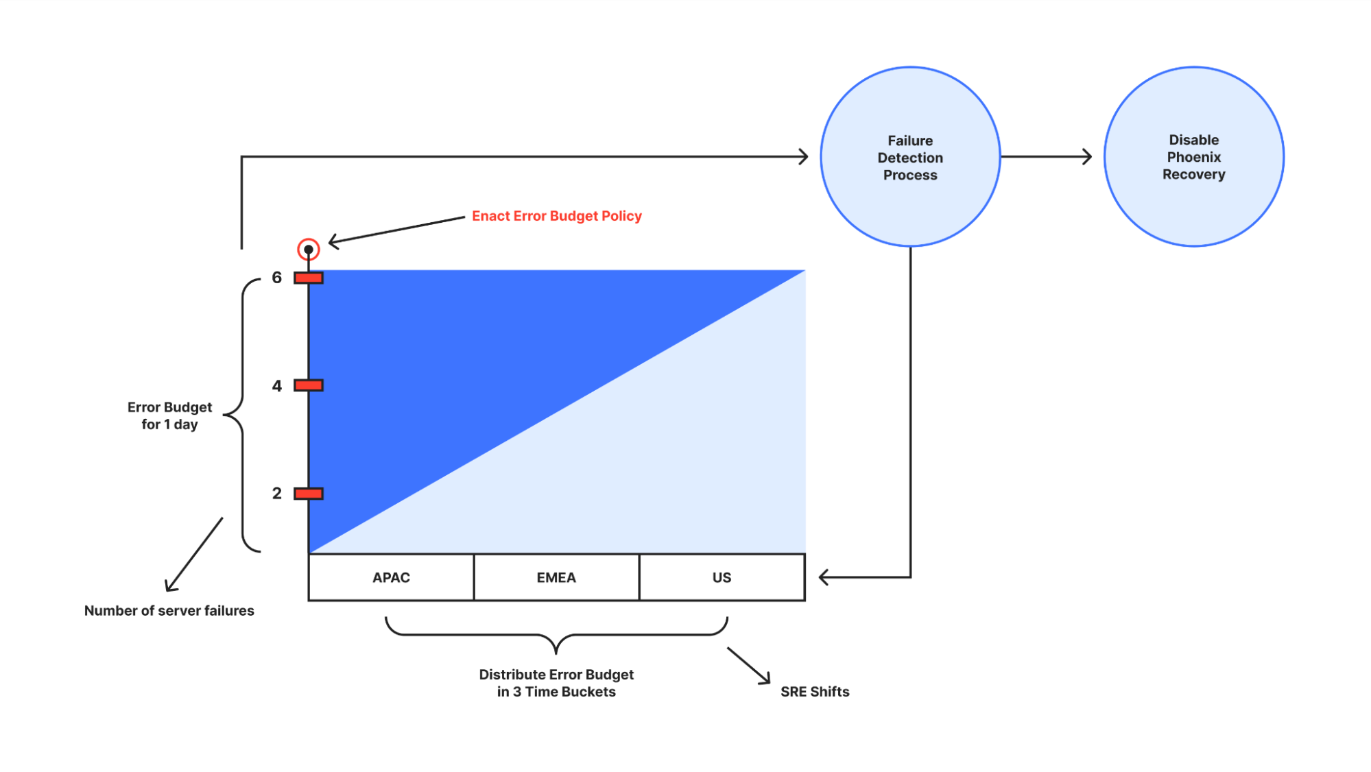
Balancing automation and empathy: Error Budgets
When we launched Phoenix, we were well aware that not every broken server can be re-enabled and successfully returned to production, and more importantly, there’s no 100% guarantee that a recovered server will be as stable as the ones with no repair history – there’s a risk that these servers could fail and end up back in Repair status again.
Although there’s no guarantee that these recovered servers won’t fail again, causing additional work for SRE’s due to the monitoring alerts that get triggered, what we can guarantee is that Phoenix immediately stops recoveries without any human intervention if a certain number of failures for a server are reached in a given time window – this is where we applied the concept of an Error Budget.
The Error Budget is the amount of error that automation can accumulate over a certain period of time before our SRE’s start being unhappy due to the excessive server failures or unreliability of the system. It is empathy embedded in automation.
In the figure above, the y-axis represents the error budget. In this context, the error budget applies to the number of recovered servers that failed and were moved back to Repair state again. The x-axis represents the time unit allocated to the error budget – in this case, 24 hours. To ensure that Phoenix is strict enough in mitigating possible issues, we divide the time unit into three consecutive buckets of the same duration – representing the three “follow the sun” SRE shifts in a day. With this, Phoenix can only execute recoveries if the number of server failures is no more than 2. Additionally, Phoenix will also have to compensate succeeding time buckets by deducting the error budget of any excess failures in a given time bucket.
Phoenix will immediately stop recoveries if it exhausts its error budget prematurely. In this context, prematurely means before the end of the time unit for which the error budget was granted. Regardless of the error budget depletion rate within a time unit, the error budget is fully replenished at the beginning of each time unit, meaning the budget resets every day.
The Error Budget has helped us define and manage our tolerance for hardware failures without causing significant harm to the system or too much noise for SREs, and gave us opportunities to improve our diagnostics system. It provides a common incentive that allows both the Infrastructure Engineering and SRE teams to focus on finding the right balance between innovation and reliability.
Where we go from here
With Phoenix, we’ve not only witnessed the significant and far-reaching potential of having an autonomous automated system in our infrastructure, we’re actually reaping its benefits as well. It provides a win-win situation by successfully recovering hardware and ensuring that broken devices are powered off, thus preventing them from consuming unnecessary power while being idle in our racks. This not only reduces energy wastage but also contributes to sustainability efforts and cost savings. Automated processes that operate independently have not only freed our colleagues on various Infrastructure teams from doing mundane and repetitive tasks, allowing them to focus more on areas where they can use their skill sets for more interesting and productive work, but have also led us to evolving our old processes for handling hardware failures and repairs, making us much more efficient than ever.
Autonomous automation is a reality that is now beginning to shape the future of how we are building better and smarter systems here at Cloudflare, and we will continue to invest engineering time for these initiatives.
A huge thank you to Elvin Tan for his awesome work on INAT, and to Graeme, Darrel and David for INAT’s continuous improvements.
As Cloudflare continues to grow, we are constantly provisioning new servers, data centers, and hardware all over the globe. With this increase in scale it became necessary to re-evaluate our approach to node and datacenter tooling. In this blog post, we explore an in-house infrastructure system we’ve built, called Zinc, to stepup to the task. This system, built in Rust, has become an essential part of system engineering, platform management, and provisioning at Cloudflare, while providing user-friendly engineering tools and automations for Cloudflare employees to leverage.
The nature of Zinc is a rather simple system, providing first class data models for logical and physical infrastructure assets here at Cloudflare. Items such as servers (nodes), network devices, and data centers are all members of Zinc, modeled in a strongly-typed system. With these models, Zinc enables powerful APIs, integrations, and interfaces for efficient fleet management on top of this data. Tasks such as assigning workloads to nodes, scheduling any type of data center maintenance, querying data about our fleet, or even managing the repair cycle of faulty nodes are greatly simplified through Zinc and its integrations with other Cloudflare systems.
By providing Cloudflare engineers with a native web interface and command line tooling for interacting with Zinc’s data, a central pane of a glass has been created, where the ability to expand, build, and monitor our fleet has never been easier.
Humble Beginnings
Several years ago, workload management and server provisioning was a tedious process. For our control plane data centers, we would define the workload for every node in massive source-controlled YAML files, sometimes as long as 80,000 lines. Each entry was a node, its name, its rack, and roles to be read by our configuration management software for assignment.
compute5545:
    rack: 219
    clickhouse:
      cluster: dns
    comment: |-
      Updated by <user>
As time went on, this became extremely cumbersome for engineers to manage and assign workloads for servers. Engineers would often have to update multiple files, updating every entry to assign and change workload data by hand. While this may seem like a slight inconvenience at first, when provisioning new hardware or changing workload configuration data, engineers would have to update hundreds of lines of YAML. Additionally, this data was not readily accessible to other systems and automation to read and modify. It became clear that this pattern could not scale, and a stronger framework would need to be created to manage this information.
First, we aimed to tackle this problem by making nodes and their workloads — which we call roles — first class data structures. Workload and node information were collected and stored in this new system called Zinc, and our configuration management system Salt began to read this information not from the YAML files, but a new RESTful API. We also added several features to Zinc to administer and manage node data:
Workload Management – Zinc assumed the role of the source of truth for node workloads, also taking charge of metadata management for roles. Attributes like a node’s associated cluster or its designated kernel version are now managed through Zinc, eliminating the need for lengthy configuration files scattered across our repositories.
Least-Privilege User Accounts – Leveraging Cloudflare Access, every Cloudflare employee who uses Zinc has an individual account, with scoped permissions for their job role. This prevents potentially compromised or prying users from viewing sensitive asset information, and makes modifications to production systems impossible without approval.
Change Request and Approval System – Zinc implements a change request system, similar to pull requests, so nodes and their associated workloads require approval from the team that manages the workload. For example, if a Cloudflare engineer wanted to provision and assign new Kubernetes nodes, this action would require approval by the Kubernetes team before being applied.
Node Reservations – It can become necessary for Cloudflare engineers to reserve specific hardware for testing and future workload capacity. Zinc provides this functionality as a first-class operation, providing a clear view into what a node is being used for, even when not in production. A common pattern to see is spare hardware for roles like Postgres or Clickhouse reserved and ready to take over if other nodes need to be taken out of production.
Node Metadata – Zinc collects a variety of node asset data through other subsystems at Cloudflare, unifying it all under a single pane of glass. Hardware information such as CPU, memory, generation, chassis, power, and networking configuration are all members of Zinc’s APIs and interfaces.
These were the initial features Zinc offered to Cloudflare’s SRE teams, but over time needs grew to expand the scope and start handling a variety of asset and operational data. Zinc has since started representing and managing more infrastructure related to network devices and datacenter management.
System Blueprint
At Cloudflare, two critical systems, Zinc and Netbox, play complementary roles in managing infrastructure. Zinc specializes in handling the logical infrastructure and operational configuration, while Netbox focuses on physical infrastructure. For those unfamiliar with Netbox, it plays the important role of acting as our Datacenter Inventory Management System (DCIM). Details such as hardware specifications, serial numbers, cable diagrams, and rack layouts are all stored in Netbox. These elements are the building blocks of the infrastructure that Zinc imports and relies on to create higher level abstractions, useful for a variety of systems on Cloudflare to depend on, without having to know the nitty-gritty specifics of our datacenter information.
Supercharged Automations
Growing pains were inevitable given the sheer pace of Cloudflare’s growth. Processes around server provisioning, maintenance windows, repairs, and diagnostics reporting were reaching their limits. Luckily, the data available through Zinc made it a natural home for new and improved workflow automations aimed at removing toil across various touch points throughout a server’s lifecycle.
Repairs Hardware failures are common at our scale. Issues such as disk failure, motherboard problems, or CPU voltage errors are just a few of the many common failures seen in production. While Cloudflare’s infrastructure is very fault tolerant, we want to quickly return hardware to production after a failure to increase capacity and optimize infrastructure costs. Prior to Zinc, engineers would have to manually collect and file tickets with information related to the hardware failure, tediously filling ticket details manually in order for data center technicians to service it. With Zinc, however, the process of collecting this data and generating repair tickets is entirely automated. As we continue developing Zinc, we will be able to manage this process all the way down to the individual hardware component level and enhance existing automation and diagnostic integrations, further optimizing the repair process. With just a few clicks (or driven by other automation), an accurate service ticket can be filed, enabling data center technicians to make repairs and get servers back into production as fast as possible.
Diagnostic Reports
Zinc integrates directly with a diagnostic service we use to identify hardware issues on our fleet, known as INAT (Integrated Node Acceptance Tests). Zinc leverages this system to run acceptance tests before, during, and after server provisioning. It also can be executed in an ad hoc manner to determine the health of a machine. With INAT, we are able to save engineers time and quickly get results back to aid in the debugging process. Once these diagnostics are complete, the Zinc interface provides a report that can be used to determine the health of a server and if any actions need to be taken.
Maintenance Windows
If you’ve ever wondered how the maintenance page on Cloudflare Status is populated, Zinc is the place of origin. As we are constantly doing hardware and network upgrades, it’s important for Cloudflare to have a centralized view of what maintenance is happening, where it is happening, and the scale of all the systems and services that are or can be impacted by the maintenance. During maintenance, there are a variety of automated systems that ensure that Cloudflare sees no loss in quality of service, no matter where in the world the maintenance is happening. Zinc orchestrates and tracks these maintenance windows, and sends alerts to teams and Cloudflare customers when a disruptive, or even potentially disruptive, maintenance is scheduled in a region.
Reboots Zinc provides an integration with a core system responsible for scheduling node reboots. When a node needs to be rebooted, such as to apply a new firmware upgrade or new Kernel version, there are systems at Cloudflare that schedule and safely manage this functionality. For example, it would be unsafe to reboot a production Clickhouse node with no prior warning, so these systems ensure traffic is properly routed away from this node prior to its reboot. Zinc provides an integration in its Web UI and CLI with this reboot management system to make the process of queuing and executing reboots much easier, as well as providing a place where we can add orchestration logic that leverages Zinc’s operational management capabilities for server reboots.
Engineer Productivity
One of the most valuable parts of Zinc is that it provides engineers the ability to quickly perform complex queries and apply changes to our assets in production. At the API layer, we ensure that any access or changes to our infrastructure are properly scoped and authenticated. From there, Zinc provides two interfaces for employees managing our fleet: a command-line interface built in Rust, and a web application built in React, both of which are built on the same Zinc API that can be directly called from scripts or other systems as integrations are built out to automate more of the management of our infrastructure.
Here are some common examples of the CLI tooling our engineers use:
# List all datacenters at Cloudflare
$ zinc site get --all
# Set a node's status to disabled, removing it from production.
$ zinc node update status compute5545 disabled
# Querying all nodes in a specific rack, that are Kubernetes nodes.
$ zinc node get -f "rack:A413" -f “role:kubernetes”
# Putting a node failure into a repair state with debug information on how to fix.
$ zinc repair node create –name 36com360 --repair-type motherboard –remove-from-prod –comments “Diagnostic determined bad motherboard”
While these are simple queries, Zinc also provides its own query syntax to get more detailed information using its own query structure. Here we see an example of looking for Kubernetes workers that are a part of our pdx cluster, while ignoring storage and rook nodes.
zinc node get -f 'role:kubernetes.cluster=pdx&kubernetes.worker=true&!kubernetes.storage&!kubernetes.rook'
Node Name    Node Type  Node Status  Colo ID  Colo Name  Rack  Rack Unit  Roles
compute2712  compute     V           348      pdx05      B103  39         kubernetes
compute1995  compute     V           349      pdx06      A104  7          kubernetes
compute1192  compute     V           36       pdx01      A203  10         kubernetes
…
Total records: 1337
Web UI Despite being an internal tool, we felt it necessary to ensure that the UX of Zinc was intuitive and crisp. As it stands, hundreds of engineers at Cloudflare rely on Zinc’s web interface, so we found it essential to provide a fast, easy to use design. Built in React as a single page application, we aim to optimize for ease of use wherever possible. Querying items such as assets in repair, nodes in a specific city or country, or even CPU model are all first-class searchable items in our UI.
As mentioned previously, Zinc also provides a user-friendly Change Request interface, similar to Git Pull Requests, which shows what asset data is changing and who is making the change, and ensures the change is approved by designated staff prior to being applied in production.
Looking Ahead
Zinc represents a significant advancement in infrastructure management at Cloudflare. With our fleet growing faster than ever, especially with our new expansions to deliver GPUs on the Edge and Cloudflare’s R2, Zinc has stepped up to the plate, tackling the challenges of growth and providing invaluable support to our engineering teams. We hope this has been an insightful view of how Cloudflare is building to grow and scale well into the future.
There are still many wins to be had when it comes to infrastructure tooling here at Cloudflare. In the long term, Zinc will continue to be the backbone of infrastructure and asset data, with deeper automations and integrations to save our engineers time and toil and reduce manual errors as we continue to expand.
If managing and operating a fleet of servers as large as Cloudflare sounds like an exciting challenge to you, we’re hiring!
Historically, data center servers have used motherboards that included all key components on a single circuit board. The DC-SCM (Datacenter-ready Secure Control Module) decouples server management and security functions from a traditional server motherboard, enabling development of server management and security solutions independent of server architecture. It also provides opportunities for reducing server printed circuit board (PCB) material cost, and allows unified firmware images to be developed.
Today, Cloudflare is announcing that it has partnered with Lenovo to design a DC-SCM for our next-generation servers. The design specification has been published to the OCP (Open Compute Project) contribution database under the name Project Argus.
A brief introduction to baseboard management controllers
A baseboard management controller (BMC) is a specialized processor that can be found in virtually every server product. It allows remote access to the server through a network connection, and provides a rich set of server management features. Some of the commonly used BMC features include server power management, device discovery, sensor monitoring, remote firmware update, system event logging, and error reporting.
In a typical server design, the BMC resides on the server motherboard, along with other key components such as the processor, memory, CPLD and so on. This was the norm for generations of server products, but that has changed in recent years as motherboards are increasingly optimized for high-speed signal bandwidth, and servers need to support specialized security requirements. This has made it necessary to decouple the BMC and its related components from the server motherboard, and move them to a smaller common form factor module known as the Datacenter Secure Control Module (DC-SCM).
Figure 1 is a picture of a motherboard used on Cloudflare’s previous generation of edge servers. The BMC and its related circuit components are placed on the same printed circuit board as the host CPU.
Figure 1: Previous Generation Server Motherboard
For Cloudflare’s next generation of edge servers, we are partnering with Lenovo to create a DC-SCM based design. On the left-hand side of Figure 2 is the printed circuit board assembly (PCBA) for the Host Processor Module (HPM). It hosts the CPU, the memory slots, and other components required for the operation and features of the server design. But the BMC and its related circuits have been relocated to a separate PCBA, which is the DC-SCM.
Figure 2: Next Generation HPM and DC-SCM
Benefits of DC-SCM based server design
PCB cost reduction
As of today, DDR5 memory runs at 6400MT/s (mega transfers per second). In the future DDR5 speed may even increase to 7200MT/s or 8800MT/s. Meanwhile, PCIe Gen5 is running at 32 GT/s (giga transfers per second), doubling the speed rate of PCIe Gen4. Both DDR5 and PCIE Gen5 are key interfaces for the processors used on our next-generation servers.
The increasing rates of high-speed IO signals and memory buses are pushing the next generation of server motherboard designs to transition from low-loss to ultra-low loss dielectric printed circuit board (PCB) materials, and higher layer counts in the PCB. At the same time, the speed of BMC and its related circuitry are not progressing so quickly. For example, the physical layer interface of ASPEED AST2600 BMC is only at PCIe Gen2 (5 GT/s).
Ultra-low loss dielectric PCB material and higher PCB layer count are both driving factors for higher PCB cost. Another driving factor of PCB cost is the size of the PCB. In a traditional server motherboard design, the size of the server motherboard is larger, since the BMC and its related circuits are placed on the same PCB as the host CPU.
By decoupling the BMC and its related circuitry from the host processor module (HPM), we can reduce the size of the relatively more expensive PCB for the HPM. BMC and its related circuitry can be placed on relatively cheaper PCB, with reduced layer count and lossier PCB dielectric materials. For example, in the design of Cloudflare’s next generation of servers, the server motherboard PCB needs to be 14 or more layers, whereas the BMC and its related components can be easily routed with 8 or 10 layers of PCB. In addition, the dielectric material used on DC-SCM PCB is low-loss dielectric — another cost saver compared to ultra-low loss dielectric materials used on HPM PCB.
Modularized design enables flexibility
DC-SCM modularizes server management and security components into a common add-in card form factor, enabling developers to remove customer specific solutions from the more complex components, such as motherboards, to the DC-SCM. This provides flexibility for developers to offer multiple customer-specific solutions, without the need to redesign multiple motherboards for each solution.
Developers are able to reuse the DC-SCM from a previous generation of server design, if the management and security requirements remain the same. This reduces the overall cost of upgrading to a new generation of servers, and has the potential to reduce e-waste when a server is decommissioned.
Likewise, management and security solution upgrades within a server generation can be carried out separately by modifying or replacing the DC-SCM. The more complex components on the HPM do not need to be redesigned. From a data center perspective, it speeds up the upgrade of management and security hardware across multiple server platforms.
Unified interoperable OpenBMC firmware development
Data center secure control interface (DC-SCI) is a standardized hardware interface between DC-SCM and the Host Processor Module (HPM). It provides a basis for electrical interoperability between different DC-SCM and host processor module (HPM) designs.
This interoperability makes it possible to have a unified firmware image across multiple DC-SCM designs, concentrating development resources on a single firmware rather than an array of them. The publicly-accessible OpenBMC repository provides a perfect platform for firmware developers of different companies to collaborate and develop such unified OpenBMC images. Instead of maintaining a separate BMC firmware image for each platform, we now use a single image that can be applied across multiple server platforms. The device tree specific to each respective server is automatically loaded based on device product information.
Using a unified OpenBMC image significantly simplifies the process of releasing BMC firmware to multiple server platforms. Firmware updates and changes are propagated to all supported platforms in a single firmware release.
Project Argus
The DC-SCM specifications have been driven by the Open Compute Project (OCP) Foundation hardware management workstream, as a way to standardize server management, security, and control features.
Cloudflare has partnered with Lenovo on what we call Project Augus, Cloudflare’s first DC-SCM implementation that fully adheres to the DC-SCM 2.0 specification. In the DC-SCM 2.0 specifications, a few design items are left open for implementers to decide on the most suitable architectural choices. With the goal of improving interoperability of Cloudflare DC-SCM designs across server vendors and server designs, Project Argus includes documentation on implementation details and design decisions on form factor, mechanical locking mechanism, faceplate design, DC-SCI pin out, BMC chip, BMC pinout, Hardware Root of Trust (HWRoT), HWRoT pinout, and minimum bootable device tree.
Figure 3: Project Argus DC-SCM 2.0
At the heart of the Project Argus DC-SCM is the ASPEED AST2600 BMC System on Chip (SoC), which when loaded with a compatible OpenBMC firmware, provides a rich set of common features necessary for remote server management. ASPEED AST1060 is used on Project Argus DC-SCM as the HWRoT solution, providing secure firmware authentication, firmware recovery, and firmware update capability. Project Argus DC-SCM 2.0 uses Lattice MachXO3D CPLD with secure boot and dual boot ability as the DC-SCM CPLD to support a variety of IO interfaces including LTPI, SGPIO, UART and GPIOs.
The mechanical form factor of Project Argus DC-SCM 2.0 is the horizontal External Form Factor (EFF).
Mechanical Drawings PDF files, including card assembly drawing and interlock rail drawing
The security foundation for our Gen 12 hardware
Cloudflare has been innovating around server design for many years, delivering increased performance per watt and reduced carbon footprints. We are excited to integrate Project Argus DC-SCM 2.0 into our next-generation, Cloudflare Gen 12 servers. Stay tuned for more exciting updates on Cloudflare Gen 12 hardware design!
Google Project Zero revealed a new flaw in AMD's Zen 2 processors in a blog post today. The 'Zenbleed' flaw affects the entire Zen 2 product stack, from AMD's EPYC data center processors to the Ryzen 3000 CPUs, and can be exploited to steal sensitive data stored in the CPU, including encryption keys and login credentials. The attack can even be carried out remotely through JavaScript on a website, meaning that the attacker need not have physical access to the computer or server.
Cloudflare’s network includes servers using AMD’s Zen line of CPUs. We have patched our entire fleet of potentially impacted servers with AMD’s microcode to mitigate this potential vulnerability. While our network is now protected from this vulnerability, we will continue to monitor for any signs of attempted exploitation of the vulnerability and will report on any attempts we discover in the wild. To better understand the Zenbleed vulnerability, read on.
Background
Understanding how a CPU executes programs is crucial to comprehending the attack's workings. The CPU works with an arithmetic processing unit called the ALU. The ALU is used to perform mathematical tasks. Operations like addition, multiplication, and floating-point calculations fall under this category. The CPU's clock signal controls the application-specific digital circuitry that the ALU uses to carry out these functions.
For data to reach the ALU, it has to pass through a series of storage systems. These include secondary memory, primary memory, cache memory, and CPU registers. Since the registers of the CPU are the target of this attack, we will go into a little more depth. Depending on the design of the computer, the CPU registers can store either 32 or 64 bits of information. The ALU can access the data in these registers and complete the operation.
As the demands on CPUs have increased, there has been a need for faster ways to perform calculations. Advanced Vector Extensions (or AVX) were developed to speed up the processing of large data sets by applications. AVX are extensions to the x86 instruction set architecture, which are relevant to x86-based CPUs from Intel and AMD. With the help of compatible software and the extra instruction set, compatible processors could handle more complex tasks. The primary motivation for developing this instruction set was to speed up operations associated with data compression, image processing, and cryptographic computations.
The vector data used by AVX instructions is stored in 16 YMM registers, each of which is 256 bits in size. The Y-register in the XMM register set is where the 128-bit values are stored, hence the name. Instructions from the arithmetic, logic, and trigonometry families of the AVX standard all make use of the YMM registers. They can also be used to keep masks, data that is used to filter out certain vector components.
Vectorized operations can be executed with great efficiency using the YMM registers. Applications that process large amounts of data stand to gain significantly from them, but they are increasingly the focus of malicious activity.
The attack
Speculative execution attacks have previously been used to compromise CPU registers. These are an attack variant that takes advantage of the speculative execution capabilities of modern CPUs. Computer processors use a method called speculative execution to speed up processing times. A CPU will execute an instruction speculatively if it has no way of knowing whether or not it will be executed. If it turns out that the CPU was unable to carry out the instruction, it will simply discard the data.
Because of their potential use for storing private information, AVX registers are especially susceptible to these kinds of attacks. Cryptographic keys and passwords, for instance, could be accessed by an attacker via a speculative execution attack on the AVX registers.
As mentioned above, Project Zero discovered a vulnerability in AMD's Zen 2-architecture-based CPUs, wherein data from another process and/or thread could be stored in the YMM registers, a 256-bit series of extended registers, potentially allowing an attacker access to sensitive information. This vulnerability is caused by a register not being written to 0 correctly under specific microarchitectural circumstances. Although this error is associated with speculative execution, it is not a side channel vulnerability.
This attack works by manipulating register files to force a mispredicted command. First, there is a trigger to XMM Register Merge Optimization2, which ironically is a hardware mitigation that can be used to protect against speculative execution attacks, followed by a register remapping (a technique used in computer processor design to resolve name conflicts between physical registers and logical registers) and then a mispredicted instruction call to vzeroupper, an instruction that is used to zero the upper half of the YMM and ZMM registers.
Since the register file is shared by all the processes running on the same physical core, this exploit can be used to eavesdrop on even the most fundamental system operations by monitoring the data being transferred between the CPU and the rest of the computer.
Fixing the bleed
Because of the exact timing for this to successfully execute, this vulnerability, CVE-2023-20593, is classified with a CVSS score of 6.5 (Medium). AMD's mitigation is implemented via the MSR register, which turns off a floating point optimization that otherwise would have allowed a move operation.
The following microcode updates have applied to our entire server fleet that contain potentially affected AMD Zen processors. We have seen no evidence of the bug being exploited and were able to patch our entire network within hours of the vulnerability’s disclosure. We will continue to monitor traffic across our network for any attempts to exploit the bug and report on our findings.
When shopping for DDR4 memory modules, we typically look at the memory density and memory speed. For example a 32GB DDR4-2666 memory module has 32GB of memory density, and the data rate transfer speed is 2666 mega transfers per second (MT/s).
If we take a closer look at the selection of DDR4 memories, we will then notice that there are several other parameters to choose from. One of them is rank x organization, for example 1Rx8, 2Rx4, 2Rx8 and so on. What are these and does memory module rank and organization have an effect on DDR4 module performance?
In this blog, we will study the concepts of memory rank and organization, and how memory rank and organization affect the memory bandwidth performance by reviewing some benchmarking test results.
Memory rank
Memory rank is a term that is used to describe how many sets of DRAM chips, or devices, exist on a memory module. A set of DDR4 DRAM chips is always 64-bit wide, or 72-bit wide if ECC is supported. Within a memory rank, all chips share the address, command and control signals.
The concept of memory rank is very similar to memory bank. Memory rank is a term used to describe memory modules, which are small printed circuit boards with memory chips and other electronic components on them; and memory bank is a term used to describe memory integrated circuit chips, which are the building blocks of the memory modules.
A single-rank (1R) memory module contains one set of DRAM chips. Each set of DRAM chips is 64-bits wide, or 72-bits wide if Error Correction Code (ECC) is supported.
A dual-rank (2R) memory module is similar to having two single-rank memory modules. It contains two sets of DRAM chips, therefore doubling the capacity of a single-rank module. The two ranks are selected one at a time through a chip select signal, therefore only one rank is accessible at a time.
Likewise, a quad-rank (4R) memory module contains four sets of DRAM chips. It is similar to having two dual-rank memories on one module, and it provides the greatest capacity. There are two chip select signals needed to access one of the four ranks. Again, only one rank is accessible at a time.
Figure 1 is a simplified view of the DQ signal flow on a dual-rank memory module. There are two identical sets of memory chips: set 1 and set 2. The 64-bit data I/O signals of each memory set are connected to a data I/O module. A single bit chip select (CS_n) signal controls which set of memory chips is accessed and the data I/O signals of the selected set will be connected to the DQ pins of the memory module.
Figure 1: DQ signal path on a dual rank memory module
Dual-rank and quad-rank memory modules double or quadruple the memory capacity on a module, within the existing memory technology. Even though only one rank can be accessed at a time, the other ranks are not sitting idle. Multi-rank memory modules use a process called rank interleaving, where the ranks that are not accessed go through their refresh cycles in parallel. This pipelined process reduces memory response time, as soon as the previous rank completes data transmission, the next rank can start its transmission.
On the other hand, there is some I/O latency penalty with multi-rank memory modules, since memory controllers need additional clock cycles to move from one rank to another. The overall latency performance difference between single rank and multi-rank memories depend heavily on the type of application.
In addition, because there are less memory chips on each module, single-rank modules produce less heat and are less likely to fail.
Memory depth and width
The capacity of each memory chip, or device, is defined as memory depth x memory width. Memory width refers to the width of the data bus, i.e. the number of DQ lines of each memory chip.
The width of memory chips are standard, they are either x4, x8 or x16. From here, we can calculate how many memory chips are in a 64-bit wide single rank memory. For example, with x4 memory chips, we will need 16 pieces (64 ÷ 4 = 16); and with x8 memory chips, we will only need 8 of them.
Let’s look at the following two high-level block diagrams of 1Gbx8 and 2Gbx4 memory chips. The total memory capacity for both of them is 8Gb. Figure 2 describes the 1Gb x8 configuration, and Figure 3 describes the 2Gbx4 configuration. With DDR4, both x4 and x8 devices have 4 groups of 4 banks. x16 devices have 2 groups of 4 banks.
We can think of each memory chip as a library. Within that library, there are four bank groups, which are the four floors of the library. On each floor, there are four shelves, each shelf is similar to one of the banks. And we can locate each one of the memory cells by its row and column addresses, just like the library book call numbers. Within each bank, the row address MUX activates a line in the memory array through the Row address latch and decoder, based on the given row address. This line is also called the word line. When a word line is activated, the data on the word line is loaded on to the sense amplifiers. Subsequently, the column decoder accesses the data on the sense amplifier based on the given column address.
Figure 2: 1Gbx8 block diagram
The capacity, or density of a memory chip is calculated as:
Memory Depth = Number of Rows * Number of Columns * Number of Banks
Total Memory Capacity = Memory Depth * Memory Width
In the example of a 1Gbx8 device as shown in Figure 2 above:
Figure 3 describes the function block diagram of a 2 Gb x 4 device.
Figure 3: 2Gbx4 Block Diagram
Number of Row Address Bits = 17
Total Number of Rows = 2 ^ 17 = 131072
Number of Column Address Bits = 10
Total Number of Columns = 2 ^ 10 = 1024
And the calculation goes:
Memory Depth = 131072 * 1024 * 16 = 2Gb
Total Memory Capacity = 2Gb* 4 = 8Gb
Memory module capacity
Memory rank and memory width determine how many memory devices are needed on each memory module.
A 64-bit DDR4 module with ECC support has a total of 72 bits for the data bus. Of the 72 bits, 8 bits are used for ECC. It would require a total of 18 x4 memory devices for a single rank module. Each memory device would supply 4 bits, and the total number of bits with 18 devices is 72 bits. For a dual rank module, we would need to double the amount of memory devices to 36.
If each x4 memory device has a memory capacity of 8Gb, a single rank module with 16 + 2 (ECC) devices would have 16GB module capacity.
8Gb * 16 = 128Gb = 16GB
And a dual rank ECC module with 36 8Gb (2Gb x 4) devices would have 32GB module capacity.
8Gb * 32 = 256Gb = 32GB
If the memory devices are x8, a 64-bit DDR4 module with ECC support would require a total of 9 x8 memory devices for a single rank module, and 18 x8 memory devices for a dual rank memory module. If each of these x8 memory devices has a memory capacity of 8Gb, a single rank module would have 8GB module capacity.
8Gb * 8 = 64Gb = 8GB
A dual rank ECC module with 18 8Gb (1Gb x 8) devices would have 16GB module capacity.
8Gb * 16 = 128Gb = 16GB
Notice that within the same memory device technology, for example 8Gb in our example, higher memory module capacity is achieved through using x4 device width, or dual-rank, or even quad-rank.
ACTIVATE timing and DRAM page sizes
Memory device width, whether it is x4, x8 or x16, also has an effect on memory timing parameters such as tFAW.
tFAW refers to Four Active Window time. It specifies a timing window within which four ACTIVATE commands can be issued. An ACTIVATE command is issued to open a row within a bank. In the block diagrams above we can see that each bank has its own set of sense amplifiers, thus one row can remain active per bank. A memory controller can issue four back-to-back ACTIVATE commands, but once the fourth ACTIVATE is done, the fifth ACTIVATE cannot be issued until the tFAW window expires.
The table below lists out the tFAW window lengths assigned to various DDR4 speeds and page sizes. Notice that under the same DDR4 speed, the bigger the page size, the longer the tFAW window is. For example, DDR4-1600 has a tFAW window of 20ns with 1/2KB page size. This means that within a bank, once a command to open a first row is issued, the controller must wait for 20ns, or 16 clock cycles (CK) before a command to open a fifth row can be issued.
The JEDEC memory standard specification for DDR4 tFAW timing varies by page sizes: 1/2KB, 1KB and 2KB.
Symbol
DDR4-1600
DDR4-1866
DDR4-2133
DDR4-2400
Four ACTIVATE windows for 1/2KB page size (minimum)
tFAW (1/2KB)
greater of 16CK or 20ns
greater of 16CK or 17ns
greater of 16CK or 15ns
greater of 16CK or 13ns
Four ACTIVATE windows for 1KB page size (minimum)
tFAW (1KB)
greater of 20CK or 25ns
greater of 20CK or 23ns
greater of 20CK or 21ns
greater of 20CK or 21ns
Four ACTIVATE windows for 2KB page size (minimum)
tFAW (2KB)
greater of 28CK or 35ns
greater of 28CK or 30ns
greater of 28CK or 30ns
greater of 28CK or 30ns
What is the relationship between page sizes and memory device width? Since we briefly compared two 8Gb memory devices earlier, it makes sense to take another look at those two in terms of page sizes.
Page size is the number of bits loaded into the sense amplifiers when a row is activated. Therefore page size is directly related to the number of bits per row, or number of columns per row.
Page Size = Number of Columns * Memory Device Width = 1024 * Memory Device Width
The table below shows the page sizes for each device width:
Device Width
Page Size (Kb)
Page Size (KB)
x4
4 Kb
1/2 KB
x8
8 Kb
1 KB
x16
16 Kb
2 KB
Among the three device widths, x4 devices have the shortest tFAW timing limit, and x16 devices have the longest tFAW timing limit. The difference in tFAW specification has a negative timing performance impact on devices with higher device width.
An experiment with 2Rx4 and 2Rx8 DDR4 modules
To quantify the impact on memory performance from different memory device widths, an experiment has been conducted on our Gen11 servers with AMD EPYC 7713 Rome CPU. The Rome CPU has 64 cores, supports 8 memory channels.
Our production Gen11 servers are configured with 1 DIMM populated in each memory channel. In order to achieve 6GB/core memory per core ratio, the total memory for the Gen11 system is 64 core * 6 GB/core = 384 GB. This is achieved by installing four pieces of 32GB 2Rx8 and four pieces of 64GB 2Rx4 memory modules.
Figure 5: Gen11 server memory configuration
To compare the bandwidth performance difference between 2Rx4 and 2Rx8 DDR4 modules, two test cases are needed. One with all 2Rx4 DDR4 modules, and another one with 2Rx8 DDR4 modules. Each test case populates eight pieces of 32GB 32Mbps DDR4 RDIMM memories in each memory channel (1DPC). As shown in the table below, the difference between the set up of the two test cases is: case A tests 2Rx4 memory modules, and case B tests 2Rx8 memory modules.
Test case
Number of DIMMs
Memory vendor
Part number
Memory size
Memory speed
Memory organization
A
8
Samsung
M393A4G43BB4-CWE
32GB
3200 MT/s
2Rx8
B
8
Samsung
M393A4K40EB3-CWECQ
32GB
3200 MT/s
2Rx4
Memory Latency Checker results
Memory Latency Checker is an Intel developed synthetic benchmarking tool. It measures memory latency and bandwidth, and how they vary with workloads of different read/write ratios, as well as stream triad. Stream triad is a memory benchmark workload that contains three operations: it first multiples a large 1D array with a scalar, then adds it to a second array, and assigns it to a third array.
2Rx8 32GB bandwidth (MB/s)
2Rx4 32GB bandwidth (MB/s)
Percentage difference
All reads
173,287
173,650
0.21%
3:1 reads-writes
154,593
156,343
1.13%
2:1 reads-writes
151,660
155,289
2.39%
1:1 reads-writes
146,895
151,199
2.93%
Stream-triad like
156,273
158,710
1.56%
The bandwidth performance difference in the All reads test case is not very significant, only 0.21%.
As the amount of writes increase, from 25% (3:1 reads-writes) to 50% (1:1 reads-writes), the bandwidth performance differences between test case A and test case B increase from 1.13% to 2.93%.
LMBench Results
LMBench is another synthetic benchmarking tool often used to study bandwidth performances of memory. Our LMBench bw_mem tests results are comparable to the results obtained from the MLC benchmark test.
2Rx8 32GB bandwidth (MB/s)
2Rx4 32GB bandwidth (MB/s)
Percentage difference
Read
170,285
173,897
2.12%
Write
73,179
76,019
3.88%
Read then write
72,804
74,926
2.91%
Copy
50,332
51,776
2.87%
The biggest bandwidth performance difference is with Write workload. The 2Rx4 test case has 3.88% higher write bandwidth than the 2Rx8 test case.
Summary
Memory organization and memory width has a slight effect on memory bandwidth performance. The difference is most obvious in write-heavy workloads than read-heavy workloads. But even in write-heavy workloads, the difference is less than 4% according to our benchmark tests.
Memory modules with x4 width require twice the number of memory devices on the memory module, as compared to memory modules with x8 width of the same capacity. More memory devices would consume more power. According to Micron’s measurement data, 2Rx8 32GB memory modules using 16Gb devices consume 31% less power than 2Rx4 32GB memory modules using 8Gb devices. The substantial power saving of using x8 memory modules may outweigh the slight bandwidth performance impact.
Our Gen11 servers are configured with a mix of 2Rx4 and 2Rx8 DDR4 modules. For our future generations, we may consider using 2Rx8 memory where possible, in order to reduce overall system power consumption, with minimal impact to bandwidth performance.
As a security company, it’s critical that we have good processes for dealing with security issues. We regularly release software to our servers – on a daily basis even – which includes new features, bug fixes, and as required, security patches. But just as critical is the software which is embedded into the server hardware, known as firmware. Primarily of interest is the BIOS and Baseboard Management Controller (BMC), but many other components also have firmware such as Network Interface Cards (NICs).
As the world becomes more digital, software which needs updating is appearing in more and more devices. As well as my computer, over the last year, I have waited patiently while firmware has updated in my TV, vacuum cleaner, lawn mower and light bulbs. It can be a cumbersome process, including obtaining the firmware, deploying it to the device which needs updating, navigating menus and other commands to initiate the update, and then waiting several minutes for the update to complete.
Firmware updates can be annoying even if you only have a couple of devices. We have more than a few devices at Cloudflare. We have a huge number of servers of varying kinds, from varying vendors, spread over 285 cities worldwide. We need to be able to rapidly deploy various types of firmware updates to all of them, reliably, and automatically, without any kind of manual intervention.
In this blog post I will outline the methods that we use to automate firmware deployment to our entire fleet. We have been using this method for several years now, and have deployed firmware without interrupting our SRE team, entirely automatically.
Background
A key component of our ability to deploy firmware at scale is the iPXE, an open source boot loader. iPXE is the glue which operates between the server and operating system, and is responsible for loading the operating system after the server has completed the Power On Self Test (POST). It is very flexible and contains a scripting language. With iPXE, we can write boot scripts which query the firmware version, continue booting if the correct firmware version is deployed, or if not, boot into a flashing environment to flash the correct firmware.
We only deploy new firmware when our systems are out of production, so we need a method to coordinate deployment only on out of production systems. The simplest way to do this is when they are rebooting, because by definition they are out of production then. We reboot our entire fleet every month, and have the ability to schedule reboots more urgently if required to deal with a security issue. Regularly rebooting our fleets has many advantages. We can deploy the latest Linux kernel, base operating system, and ensure that we do not have any breaking changes in our operating system and configuration management environment that breaks on fresh boot.
Our entire fleet operates in UEFI mode. UEFI is a modern replacement for the BIOS and offers more features and more security, such as Secure Boot. A full description of all of these changes is outside the scope of this article, but essentially UEFI provides a minimal environment and shell capable of executing binaries. Secure Boot ensures that the binaries are signed with keys embedded in the system, to prevent a bad actor from tampering with our software.
How we update the BIOS
We are able to update the BIOS without booting any operating system, purely by taking advantage of features offered by iPXE and the UEFI shell. This requires a flashing binary written for the UEFI environment.
Upon boot, iPXE is started. Through iPXE’s built-in variable ${smbios/0.5.0} it is possible to query the current BIOS version, and compare it to the latest version, and trigger a flash only if there is a mis-match. iPXE then downloads the files required for the firmware update to a ramdisk.
The following is an example of a very basic iPXE script which performs such an action:
# Check whether the BIOS version is 2.03
iseq ${smbios/0.5.0} 2.03 || goto biosupdate
echo Nothing to do for {{ model }}
exit 0

:biosupdate
echo Trying to update BIOS/UEFI...
echo Current: ${smbios/0.5.0}
echo New: 2.03

imgfetch ${boot_prefix}/tools/x64/shell.efi || goto unexpected_error
imgfetch startup.nsh || goto unexpected_error

imgfetch AfuEfix64.efi || goto unexpected_error
imgfetch bios-2.03.bin || goto unexpected_error

imgexec shell.efi || goto unexpected_error
Meanwhile, startup.nsh contains the binary to run and command line arguments to effect the flash:
After rebooting, the machine will boot using its new BIOS firmware, version 2.03. Since ${smbios/0.5.0} now contains 2.03, the machine continues to boot and enter production.
Other firmware updates such as BMC, network cards and more
Unfortunately, the number of vendors that support firmware updates with UEFI flashing binaries is limited. There are a large number of other updates that we need to perform such as BMC and NIC.
Consequently, we need another way to flash these binaries. Thankfully, these vendors invariably support flashing from Linux. Consequently we can perform flashing from a minimal Linux environment. Since vendor firmware updates are typically closed source utilities and vendors are often highly secretive about firmware flashing, we can ensure that the flashing environment does not provide an attackable surface by ensuring that the network is not configured. If it’s not on the network, it can’t be attacked and exploited.
Not being on the network means that we need to inject files into the boot process when the machine boots. We can accomplish this with an initial ramdisk (initrd), and iPXE makes it easy to add additional initrd to the boot.
Creating an initrd is as simple as creating an archive of the files using cpio using the newc archive format.
Let’s imagine we are going to flash Broadcom NIC firmware. We’ll use the bnxtnvm firmware update utility, the firmware image firmware.pkg, and a shell script called flash to automate the task.
The files are laid out in the file system like this:
cd broadcom
find .
./opt/preflight
./opt/preflight/scripts
./opt/preflight/scripts/flash
./opt/broadcom
./opt/broadcom/firmware.pkg
./opt/broadcom/bnxtnvm
Now we compress all of these files into an image called broadcom.img.
This is the first step completed; we have the firmware packaged up into an initrd.
Since it’s challenging to read, say, the firmware version of the NIC, from the EFI shell, we store firmware versions as UEFI variables. These can be written from Linux via efivars, the UEFI variable file system, and then read by iPXE on boot.
An example of writing an EFI variable from Linux looks like this:
declare -r fw_path='/sys/firmware/efi/efivars/broadcom-fw-9ca25c23-368a-4c21-943f-7d91f2b76008'
declare -r efi_header='\x07\x00\x00\x00'
declare -r version='1.05'

/bin/mount -o remount,rw,nosuid,nodev,noexec,noatime none /sys/firmware/efi/efivars

# Files on efivarfs are immutable by default, so remove the immutable flag so that we can write to it: https://docs.kernel.org/filesystems/efivarfs.html
if [ -f "${fw_path}" ] ; then
    /usr/bin/chattr -i "${fw_path}"
fi

echo -n -e "${efi_header}${version}" >| "$fw_path"
Then we can write an iPXE configuration file to load the flashing kernel, userland and flashing utilities.
set cf/guid 9ca25c23-368a-4c21-943f-7d91f2b76008

iseq ${efivar/broadcom-fw-${cf/guid}} 1.05 && echo Not flashing broadcom firmware, version already at 1.05 || goto update
exit

:update
echo Starting broadcom firmware update
kernel ${boot_prefix}/vmlinuz initrd=baseimg.img initrd=linux-initramfs-modules.img initrd=broadcom.img
initrd ${boot_prefix}/baseimg.img
initrd ${boot_prefix}/linux-initramfs-modules.img
initrd ${boot_prefix}/firmware/broadcom.img
Flashing scripts are deposited into /opt/preflight/scripts and we use systemd to execute them with run-parts on boot:
/etc/systemd/system/preflight.service:
[Unit]
Description=Pre-salt checks and simple configurations on boot
Before=salt-highstate.service
After=network.target

[Service]
Type=oneshot
RemainAfterExit=yes
ExecStart=/bin/run-parts --verbose /opt/preflight/scripts

[Install]
WantedBy=multi-user.target
RequiredBy=salt-highstate.service
An example flashing script in /opt/preflight/scripts might look like:
#!/bin/bash

trap 'catch $? $LINENO' ERR
catch(){
    #error handling goes here
    echo "Error $1 occured on line $2"
}

declare -r fw_path='/sys/firmware/efi/efivars/broadcom-fw-9ca25c23-368a-4c21-943f-7d91f2b76008'
declare -r efi_header='\x07\x00\x00\x00'
declare -r version='1.05'

lspci | grep -q Broadcom
if [ $? -eq 0 ]; then
    echo "Broadcom firmware flashing starting"
    if [ ! -f "$fw_path" ] ; then
        chmod +x /opt/broadcom/bnxtnvm
        declare -r interface=$(/opt/broadcom/bnxtnvm listdev | grep "Device Interface Name" | awk -F ": " '{print $2}')
        /opt/broadcom/bnxtnvm -dev=${interface} -force -y install /opt/broadcom/BCM957414M4142C.pkg
        declare -r status=$?
        declare -r currentversion=$(/opt/broadcom/bnxtnvm -dev=${interface} device_info | grep "Package version on NVM" | awk -F ": " '{print $2}')
        declare -r expectedversion=$(echo $version | awk '{print $2}')
        if [ $status -eq 0 -a "$currentversion" = "$expectedversion" ]; then
            echo "Broadcom firmware $version flashed successfully"
            /bin/mount -o remount,rw,nosuid,nodev,noexec,noatime none /sys/firmware/efi/efivars
            echo -n -e "${efi_header}${version}" >| "$fw_path"
            echo "Created $fw_path"
        else
            echo "Failed to flash Broadcom firmware $version"
            /opt/broadcom/bnxtnvm -dev=${interface} device_info
        fi
    else
        echo "Broadcom firmware up-to-date"
    fi
else
    echo "No Broadcom NIC installed"
    /bin/mount -o remount,rw,nosuid,nodev,noexec,noatime none /sys/firmware/efi/efivars
    if [ -f "${fw_path}" ] ; then
        /usr/bin/chattr -i "${fw_path}"
    fi
    echo -n -e "${efi_header}${version}" >| "$fw_path"
    echo "Created $fw_path"
fi

if [ -f "${fw_path}" ]; then
    echo "rebooting in 60 seconds"
    sleep 60
    /sbin/reboot
fi
Conclusion
Whether you manage just your laptop or desktop computer, or a fleet of servers, it’s important to keep the firmware updated to ensure that the availability, performance and security of the devices is maintained.
If you have a few devices and would benefit from automating the deployment process, we hope that we have inspired you to have a go by making use of some basic open source tools such as the iPXE boot loader and some scripting.
Final thanks to my colleague Ignat Korchagin who did a large amount of the original work on the UEFI BIOS firmware flashing infrastructure.
Over the last few years, there has been a rise in the number of attacks that affect how a computer boots. Most modern computers use a specification called Unified Extensible Firmware Interface (UEFI) that defines a software interface between an operating system (e.g. Windows) and platform firmware (e.g. disk drives, video cards). There are security mechanisms built into UEFI that ensure that platform firmware can be cryptographically validated and boot securely through an application called a bootloader. This firmware is stored in non-volatile SPI flash memory on the motherboard, so it persists on the system even if the operating system is reinstalled and drives are replaced.
This creates a ‘trust anchor’ used to validate each stage of the boot process, but, unfortunately, this trust anchor is also a target for attack. In these UEFI attacks, malicious actions are loaded onto a compromised device early in the boot process. This means that malware can change configuration data, establish persistence by ‘implanting’ itself, and can bypass security measures that are only loaded at the operating system stage. So, while UEFI-anchored secure boot protects the bootloader from bootloader attacks, it does not protect the UEFI firmware itself.
Because of this growing trend of attacks, we began the process of cryptographically signing our UEFI firmware as a mitigation step. While our existing solution is platform specific to our x86 AMD server fleet, we did not have a similar solution to UEFI firmware signing for Arm. To determine what was missing, we had to take a deep dive into the Arm secure boot process.
Read on to learn about the world of Arm Trusted Firmware Secure Boot.
Arm Trusted Firmware Secure Boot
Arm defines a trusted boot process through an architecture called Trusted Board Boot Requirements (TBBR), or Arm Trusted Firmware (ATF) Secure Boot. TBBR works by authenticating a series of cryptographically signed binary images each containing a different stage or element in the system boot process to be loaded and executed. Every bootloader (BL) stage accomplishes a different stage in the initialization process:
BL1
BL1 defines the boot path (is this a cold boot or warm boot), initializes the architectures (exception vectors, CPU initialization, and control register setup), and initializes the platform (enables watchdog processes, MMU, and DDR initialization).
BL2
BL2 prepares initialization of the Arm Trusted Firmware (ATF), the stack responsible for setting up the secure boot process. After ATF setup, the console is initialized, memory is mapped for the MMU, and message buffers are set for the next bootloader.
BL3
The BL3 stage has multiple parts, the first being initialization of runtime services that are used in detecting system topology. After initialization, there is a handoff between the ATF ‘secure world’ boot stage to the ‘normal world’ boot stage that includes setup of UEFI firmware. Context is set up to ensure that no secure state information finds its way into the normal world execution state.
Each image is authenticated by a public key, which is stored in a signed certificate and can be traced back to a root key stored on the SoC in one time programmable (OTP) memory or ROM.
TBBR was originally designed for cell phones. This established a reference architecture on how to build a “Chain of Trust” from the first ROM executed (BL1) to the handoff to “normal world” firmware (BL3). While this creates a validated firmware signing chain, it has caveats:
SoC manufacturers are heavily involved in the secure boot chain, while the customer has little involvement.
A unique SoC SKU is required per customer. With one customer this could be easy, but most manufacturers have thousands of SKUs
The SoC manufacturer is primarily responsible for end-to-end signing and maintenance of the PKI chain. This adds complexity to the process requiring USB key fobs for signing.
Doesn’t scale outside the manufacturer.
What this tells us is what was built for cell phones doesn’t scale for servers.
If we were involved 100% in the manufacturing process, then this wouldn’t be as much of an issue, but we are a customer and consumer. As a customer, we have a lot of control of our server and block design, so we looked at design partners that would take some of the concepts we were able to implement with AMD Platform Secure Boot and refine them to fit Arm CPUs.
Amping it up
We partnered with Ampere and tested their Altra Max single socket rack server CPU (code named Mystique) that provides high performance with incredible power efficiency per core, much of what we were looking for in reducing power consumption. These are only a small subset of specs, but Ampere backported various features into the Altra Max notably, speculative attack mitigations that include Meltdown and Spectre (variants 1 and 2) from the Armv8.5 instruction set architecture, giving Altra the “+” designation in their ISA.
Ampere does implement a signed boot process similar to the ATF signing process mentioned above, but with some slight variations. We’ll explain it a bit to help set context for the modifications that we made.
Ampere Secure Boot
The diagram above shows the Arm processor boot sequence as implemented by Ampere. System Control Processors (SCP) are comprised of the System Management Processor (SMpro) and the Power Management Processor (PMpro). The SMpro is responsible for features such as secure boot and bmc communication while the PMpro is responsible for power features such as Dynamic Frequency Scaling and on-die thermal monitoring.
At power-on-reset, the SCP runs the system management bootloader from ROM and loads the SMpro firmware. After initialization, the SMpro spawns the power management stack on the PMpro and ATF threads. The ATF BL2 and BL31 bring up processor resources such as DRAM, and PCIe. After this, control is passed to BL33 BIOS.
Authentication flow
At power on, the SMpro firmware reads Ampere’s public key (ROTPK) from the SMpro key certificate in SCP EEPROM, computes a hash and compares this to Ampere’s public key hash stored in eFuse. Once authenticated, Ampere’s public key is used to decrypt key and content certificates for SMpro, PMpro, and ATF firmware, which are launched in the order described above.
The SMpro public key will be used to authenticate the SMpro and PMpro images and ATF keys which in turn will authenticate ATF images. This cascading set of authentication that originates with the Ampere root key and stored in chip called an electronic fuse, or eFuse. An eFuse can be programmed only once, setting the content to be read-only and can not be tampered with nor modified.
This is the original hardware root of trust used for signing system, secure world firmware. When we looked at this, after referencing the signing process we had with AMD PSB and knowing there was a large enough one-time-programmable (OTP) region within the SoC, we thought: why can’t we insert our key hash in here?
Single Domain Secure Boot
Single Domain Secure Boot takes the same authentication flow and adds a hash of the customer public key (Cloudflare firmware signing key in this case) to the eFuse domain. This enables the verification of UEFI firmware by a hardware root of trust. This process is performed in the already validated ATF firmware by BL2. Our public key (dbb) is read from UEFI secure variable storage, a hash is computed and compared to the public key hash stored in eFuse. If they match, the validated public key is used to decrypt the BL33 content certificate, validating and launching the BIOS, and remaining boot items. This is the key feature added by SDSB. It validates the entire software boot chain with a single eFuse root of trust on the processor.
Building blocks
With a basic understanding of how Single Domain Secure Boot works, the next logical question is “How does it get implemented?”. We ensure that all UEFI firmware is signed at build time, but this process can be better understood if broken down into steps.
Ampere, our original device manufacturer (ODM), and we play a role in execution of SDSB. First, we generate certificates for a public-private key pair using our internal, secure PKI. The public key side is provided to the ODM as dbb.auth and dbu.auth in UEFI secure variable format. Ampere provides a reference Software Release Package (SRP) including the baseboard management controller, system control processor, UEFI, and complex programmable logic device (CPLD) firmware to the ODM, who customizes it for their platform. The ODM generates a board file describing the hardware configuration, and also customizes the UEFI to enroll dbb and dbu to secure variable storage on first boot.
Once this is done, we generate a UEFI.slim file using the ODM’s UEFI ROM image, Arm Trusted Firmware (ATF) and Board File. (Note: This differs from AMD PSB insofar as the entire image and ATF files are signed; with AMD PSB, only the first block of boot code is signed.) The entire .SLIM file is signed with our private key, producing a signature hash in the file. This can only be authenticated by the correct public key. Finally, the ODM packages the UEFI into .HPM format compatible with their platform BMC.
In parallel, we provide the debug fuse selection and hash of our DER-formatted public key. Ampere uses this information to create a special version of the SCP firmware known as Security Provisioning (SECPROV) .slim format. This firmware is run one time only, to program the debug fuse settings and public key hash into the SoC eFuses. Ampere delivers the SECPROV .slim file to the ODM, who packages it into a .hpm file compatible with the BMC firmware update tooling.
Fusing the keys
During system manufacturing, firmware is pre-programmed into storage ICs before placement on the motherboard. Note that the SCP EEPROM contains the SECPROV image, not standard SCP firmware. After a system is first powered on, an IPMI command is sent to the BMC which releases the Ampere processor from reset. This allows SECPROV firmware to run, burning the SoC eFuse with our public key hash and debug fuse settings.
Final manufacturing flow
Once our public key has been provisioned, manufacturing proceeds by re-programming the SCP EEPROM with its regular firmware. Once the system powers on, ATF detects there are no keys present in secure variable storage and allows UEFI firmware to boot, regardless of signature. Since this is the first UEFI boot, it programs our public key into secure variable storage and reboots. ATF is validated by Ampere’s public key hash as usual. Since our public key is present in dbb, it is validated against our public key hash in eFuse and allows UEFI to boot.
Validation
The first part of validation requires observing successful destruction of the eFuses. This imprints our public key hash into a dedicated, immutable memory region, not allowing the hash to be overwritten. Upon automatic or manual issue of an IPMI OEM command to the BMC, the BMC observes a signal from the SECPROV firmware, denoting eFuse programming completion. This can be probed with BMC commands.
When the eFuses have been blown, validation continues by observing the boot chain of the other firmware. Corruption of the SCP, ATF, or UEFI firmware obstructs boot flow and boot authentication and will cause the machine to fail booting to the OS. Once firmware is in place, happy path validation begins with booting the machine.
Upon first boot, firmware boots in the following order: BMC, SCP, ATF, and UEFI. The BMC, SCP, and ATF firmware can be observed via their respective serial consoles. The UEFI will automatically enroll the dbb and dbu files to the secure variable storage and trigger a reset of the system.
After observing the reset, the machine should successfully boot to the OS if the feature is executed correctly. For further validation, we can use the UEFI shell environment to extract the dbb file and compare the hash against the hash submitted to Ampere. After successfully validating the keys, we flash an unsigned UEFI image. An unsigned UEFI image causes authentication failure at bootloader stage BL3-2. The ATF firmware undergoes a boot loop as a result. Similar results will occur for a UEFI image signed with incorrect keys.
Updated authentication flow
On all subsequent boot cycles, the ATF will read secure variable dbb (our public key), compute a hash of the key, and compare it to the read-only Cloudflare public key hash in eFuse. If the computed and eFuse hashes match, our public key variable can be trusted and is used to authenticate the signed UEFI. After this, the system boots to the OS.
Let’s boot!
We were unable to get a machine without the feature enabled to demonstrate the set-up of the feature since we have the eFuse set at build time, but we can demonstrate what it looks like to go between an unsigned BIOS and a signed BIOS. What we would have observed with the set-up of the feature is a custom BMC command to instruct the SCP to burn the ROTPK into the SOC’s OTP fuses. From there, we would observe feedback to the BMC detailing whether burning the fuses was successful. Upon booting the UEFI image for the first time, the UEFI will write the dbb and dbu into secure storage.
As you can see, after flashing the unsigned BIOS, the machine fails to boot.
Despite the lack of visibility in failure to boot, there are a few things going on underneath the hood. The SCP (System Control Processor) still boots.
The SCP image holds a key certificate with Ampere’s generated ROTPK and the SCP key hash. SCP will calculate the ROTPK hash and compare it against the burned OTP fuses. In the failure case, where the hash does not match, you will observe a failure as you saw earlier. If successful, the SCP firmware will proceed to boot the PMpro and SMpro. Both the PMpro and SMpro firmware will be verified and proceed with the ATF authentication flow.
The conclusion of the SCP authentication is the passing of the BL1 key to the first stage bootloader via the SCP HOB(hand-off-block) to proceed with the standard three stage bootloader ATF authentication mentioned previously.
At BL2, the dbb is read out of the secure variable storage and used to authenticate the BL33 certificate and complete the boot process by booting the BL33 UEFI image.
Still more to do
In recent years, management interfaces on servers, like the BMC, have been the target of cyber attacks including ransomware, implants, and disruptive operations. Access to the BMC can be local or remote. With remote vectors open, there is potential for malware to be installed on the BMC via network interfaces. With compromised software on the BMC, malware or spyware could maintain persistence on the server. An attacker might be able to update the BMC directly using flashing tools such as flashrom or socflash without the same level of firmware resilience established at the UEFI level.
The future state involves using host CPU-agnostic infrastructure to enable a cryptographically secure host prior to boot time. We will look to incorporate a modular approach that has been proposed by the Open Compute Project’s Data Center Secure Control
Module Specification (DC-SCM) 2.0 specification. This will allow us to standardize our Root of Trust, sign our BMC, and assign physically unclonable function (PUF) based identity keys to components and peripherals to limit the use of OTP fusing. OTP fusing creates a problem with trying to “e-cycle” or reuse machines as you cannot truly remove a machine identity.
Today, as part of Cloudflare’s Impact Week, we’re excited to announce an opportunity for Cloudflare customers to make it easier to decommission and dispose of their used hardware appliances sustainably. We’re partnering with Iron Mountain to offer preferred pricing and discounts for Cloudflare customers that recycle or remarket legacy hardware through its service.
Replacing legacy hardware with Cloudflare’s network
Cloudflare’s products enable customers to replace legacy hardware appliances with our global network. Connecting to our network enables access to firewall (including WAF and Network Firewalls, Intrusion Detection Systems, etc), DDoS mitigation, VPN replacement, WAN optimization, and other networking and security functions that were traditionally delivered in physical hardware. These are served from our network and delivered as a service. This creates a myriad of benefits for customers including stronger security, better performance, lower operational overhead, and none of the headaches of traditional hardware like capacity planning, maintenance, or upgrade cycles. It’s also better for the Earth: our multi-tenant SaaS approach means more efficiency and a lower carbon footprint to deliver those functions.
But what happens with all that hardware you no longer need to maintain after switching to Cloudflare?
The life of a hardware box
The life of a hardware box begins on the factory line at the manufacturer. These are then packaged, shipped and installed at the destination infrastructure where they provide processing power to run front-end products or services, and routing network traffic. Occasionally, if the hardware fails to operate, or its performance declines over time, it will get fixed or will be returned for replacement under the warranty.
When none of these options work, the hardware box is considered end-of-life and it “dies”. This hardware must be decommissioned by being disconnected from the network, and then physically removed from the data center for disposal.
The useful lifespan of hardware depends on the availability of newer generations of processors which help realize critical efficiency improvements around cost, performance, and power. In general, the industry standard of hardware decommissioning timeline is between three and six years after installation. There are additional benefits to refreshing these physical assets at the lower end of the hardware lifespan spectrum, keeping your infrastructure at optimal performance.
In the instance where the hardware still works, but is replaced by newer technologies, it would be such a waste to discard this gear. Instead, there could be recoverable value in this outdated hardware. And simply tossing unwanted hardware into the trash indiscriminately, which will eventually become part of the landfill, causes devastating consequences as these electronic devices contain hazardous materials like lithium, palladium, lead, copper and cobalt or mercury, and those could contaminate the environment. Below, we explain sustainable alternatives and cost-beneficial practices one can pursue to dispose of your infrastructure hardware.
Option 1: Remarket / Reuse
For hardware that still works, the most sustainable route is to sanitize it of data, refurbish, and resell it in the second-hand market at a depreciated cost. Some IT asset disposition firms would also repurpose used hardware to maximize its market value. For example, harvesting components from a device to build part of another product and selling that at a higher price. For working parts that have very little resale value, companies can also consider reusing them to build a spare parts inventory for replacing failed parts later in the data centers.
The benefits of remarket and reuse are many. It helps maximize a hardware’s return of investment by including any reclaimed value at end-of-life stage, offering financial benefits to the business. And it reduces discarded electronics, or e-waste and their harmful efforts on our environment, helping socially responsible organizations build a more sustainable business. Lastly, it provides alternatives to individuals and organizations that cannot afford to buy new IT equipment.
Option 2: Recycle
For used hardware that is not able to be remarketed, it is recommended to engage an asset disposition firm to professionally strip it of any valuable and recyclable materials, such as precious metal and plastic, before putting it up for physical destruction. Similar to remarketing, recycling also reduces environmental impact, and cuts down the amount of raw materials needed to manufacture new products.
A key factor in hardware recycling is a secure chain of custody. Meaning, a supplier has the right certification, preferably its own fleet and secure facilities to properly and securely process the equipment.
Option 3: Destroy
From a sustainable point of view, this route should only be used as a last resort. When hardware does not operate as it is intended to, and has no remarketed nor recycled value, an asset disposition supplier would remove all the asset tags and information from it in preparation for a physical destruction. Depending on disposal policies, some companies would choose to sanitize and destroy all the data bearing hardware, such as SSD or HDD, for security reasons.
To further maximize recycling value and reduce e-waste, it is recommended to keep security policy up to date on discarded IT equipment and explore the option of reusing working devices after a professional data wiping as much as possible.
At Cloudflare, we follow an industry-standard capital depreciation timeline, which culminates in recycling actions through the engagement of IT asset disposition partners including Iron Mountain. Through these partnerships, besides data bearing hardware which follows the security policy to be sanitized and destroyed, approximately 99% of the rest decommissioned IT equipment from Cloudflare is sold or recycled.
Partnering with Iron Mountain to make sustainable goals more accessible
Hardware discomission can be a burden on a business, from operational strain to complex processes, a lack of streamlined execution to the risk of a data breach. Our experience shows that partnering with an established firm like Iron Mountain who is specialized in IT asset disposition would help kick-start one’s hardware recycling journey.
Iron Mountain has more than two decades of experience working with Hyperscale technology and data centers. A market leader in decommissioning, data security and remarketing capabilities. It has a wide footprint of facilities to support their customers’ sustainability goals globally.
Today, Iron Mountain has generated more than US$1.5 billion through value recovery and has been continually developing new ways to sell mass volumes of technology for their best use. Other than their end-to-end decommission offering, there are two additional value adding services that Iron Mountain provides to their customers that we find valuable. They offer a quarterly survey report which presents insights in the used market, and a sustainability report that measures the environmental impact based on total hardware processed with their customers.
Get started today
Get started today with Iron Mountain on your hardware recycling journey and sign up from here. After receiving the completed contact form, Iron Mountain will consult with you on the best solution possible. It has multiple programs to support including revenue share, fair market value, and guaranteed destruction with proper recycling. For example, when it comes to reselling used IT equipment, Iron Mountain would propose an appropriate revenue split, namely how much percentage of sold value will be shared with the customer, based on business needs. Iron Mountain’s secure chain of custody with added solutions such as redeployment, equipment retrieval programs, and onsite destruction can ensure it can tailor the solution that works best for your company’s security and environmental needs.
And in collaboration with Cloudflare, Iron Mountain offers additional two percent on your revenue share of the remarketed items and a five percent discount on the standard fees for other IT asset disposition services if you are new to Iron Mountain and choose to use these services via the link in this blog.
Whether you are building a global network or buying groceries, some rules of sustainable living remain the same: be thoughtful about what you get, make the most out of what you have, and try to upcycle your waste rather than throwing it away. These rules are central to Cloudflare — we take helping build a better Internet seriously, and we define this as not just having the most secure, reliable, and performant network — but also the most sustainable one.
With incredible growth of the Internet, and the increased usage of Cloudflare’s network, even linear improvements to sustainability in our hardware today will result in exponential gains in the future. We want to use this post to outline how we think about the sustainability impact of the hardware in our network, and what we’re doing to continually mitigate that impact.
Sustainability in the realm of servers
The total carbon footprint of a server is approximately 6 tons of Carbon Dioxide equivalent (CO2eq) when used in the US. There are four parts to the carbon footprint of any computing device:
The embodied emissions: source materials and production
Packing and shipping
Use of the product
End of life.
The emissions from the actual operations and use of a server account for the vast majority of the total life-cycle impact. The secondary impact is embodied emissions (which is the carbon footprint from the creation of the device in the first place), which is about 10% overall.
Use of Product Emissions
It’s difficult to reduce the total emissions for the operation of servers. If there’s a workload that needs computing power, the server will complete the workload and use the energy required to complete it. What we can do, however, is consistently seek to improve the amount of computing output per kilo of CO2 emissions — and the way we do that is to consistently upgrade our hardware to the most power-efficient designs. As we switch from one generation of server to the next, we often see very large increases in computing output, at the same level of power consumption. In this regard, given energy is a large cost for our business, our incentives of reducing our environmental impact are naturally aligned to our business model.
Embodied Emissions
The other large category of emissions — the embodied emissions — are a domain where we actually have a lot more control than the use of the product. Reminder from before: the embodied carbon means the sources of emissions generated outside of equipments’ operation. How can we reduce the embodied emissions involved in running a fleet of servers? Turns out, there are a few ways: modular design, relying on open vs proprietary standards to enable reuse, and recycling.
Modular Design
The first big opportunity is through modular system design. Modular systems are a great way of reducing embodied carbon, as they result in fewer new components and allow for parts that don’t have efficiency upgrades to be leveraged longer. Modular server design is essentially decomposing functions of the motherboard onto sub-boards so that the server owner can selectively upgrade the components that are required for their use cases.
How much of an impact can modular design have? Well, if 30% of the server is delivering meaningful efficiency gains (usually CPU and memory, sometimes I/O), we may really need to upgrade those in order to meet efficiency goals, but creating an additional 70% overhead in embodied carbon (i.e. the rest of the server, which often is made up of components that do not get more efficient) is not logical. Modular design allows us to upgrade the components that will improve the operational efficiency of our data centers, but amortize carbon in the “glue logic” components over the longer time periods for which they can continue to function.
Previously, many systems providers drove ridiculous and useless changes in the peripherals (custom I/Os, outputs that may not be needed for a specific use case such as VGA for crash carts we might not use given remote operations, etc.), which would force a new motherboard design for every new CPU socket design. By standardizing those interfaces across vendors, we can now only source the components we need, and reuse a larger percentage of systems ourselves. This trend also helps with reliability (sub-boards are more well tested), and supply assurance (since standardized subcomponent boards can be sourced from more vendors), something all of us in the industry have had top-of-mind given global supply challenges of the past few years.
Standards-based Hardware to Encourage Re-use
But even with modularity, components need to go somewhere after they’ve been deprecated — and historically, this place has been a landfill. There is demand for second-hand servers, but many have been parts of closed systems with proprietary firmware and BIOS, so repurposing them has been costly or impossible to integrate into new systems. The economics of a circular economy are such that service fees for closed firmware and BIOS support as well as proprietary interconnects or ones that are not standardized can make reuse prohibitively expensive. How do you solve this? Well, if servers can be supported using open source firmware and BIOS, you dramatically reduce the cost of reusing the parts — so that another provider can support the new customer.
Recycling
Beyond that, though, there are parts failures, or parts that are simply no longer economical to be run, even in the second hand market. Metal recycling can always be done, and some manufacturers are starting to invest in programs there, although the energy investment for extracting the usable elements sometimes doesn’t make sense. There is innovation in this domain, Zhan, et al. (2020) developed an environmentally friendly and efficient hydrothermal-buffering technique for the recycling of GaAs-based ICs, achieving gallium and arsenic recovery rates of 99.9 and 95.5% respectively. Adoption is still limited — most manufacturers are discussing water recycling and renewable energy vs. full-fledged recycling of metals — but we’re closely monitoring the space to take advantage of any further innovation that happens.
What Cloudflare is Doing To Reduce Our Server Impact
It is great to talk about these concepts, but we are doing this work today. I’d describe them as being under two main banners: taking steps to reduce embodied emissions through modular and open standards design, and also using the most power-efficient solutions for our workloads.
Gen 12: Walking the Talk
Our next generation of servers, Gen 12, will be coming soon. We’re emphasizing modular-driven design, as well as a focus on open standards, to enable reuse of the components inside the servers.
A modular-driven design
Historically, every generation of server here at Cloudflare has required a massive redesign. An upgrade to a new CPU required a new motherboard, power supply, chassis, memory DIMMs, and BMC. This, in turn, might mean new fans, storage, network cards, and even cables. However, many of these components are not changing drastically from generation to generation: these components are built using older manufacturing processes, and leverage interconnection protocols that do not require the latest speeds.
To help illustrate this, let’s look at our Gen 11 server today: a single socket server is ~450W of power, with the CPU and associated memory taking about 320W of that (potentially 360W at peak load). All the other components on that system (mentioned above) are ~100W of operational power (mostly dominated by fans, which is why so many companies are exploring alternative cooling designs), so they are not where the optimization efforts or newer ICs will greatly improve the system’s efficiency. So, instead of rebuilding all those pieces from scratch for every new server and generating that much more embodied carbon, we are reusing them as often as possible.
By disaggregating components that require changes for efficiency reasons from other system-level functions (storage, fans, BMCs, programmable logic devices, etc.), we are able to maximize reuse of electronic components across generations. Building systems modularly like this significantly reduces our embodied carbon footprint over time. Consider how much waste would be eliminated if you were able to upgrade your car’s engine to improve its efficiency without changing the rest of the parts that are working well, like the frame, seats, and windows. That’s what modular design is enabling in data centers like ours across the world.
A Push for Open Standards, Too
We, as an industry, have to work together to accelerate interoperability across interfaces, standards, and vendors if we want to achieve true modularity and our goal of a 70% reduction in e-waste. We have begun this effort by leveraging standard add-in-card form factors (OCP 2.0 and 3.0 NICs, Datacenter Secure Control Module for our security and management modules, etc.) and our next server design is leveraging Datacenter Modular Hardware System, an open-source design specification that allows for modular subcomponents to be connected across common buses (regardless of the system manufacturer). This technique allows us to maintain these components over multiple generations without having to incur more carbon debt on parts that don’t change as often as CPUs and memory.
In order to enable a more comprehensive circular economy, Cloudflare has made extensive and increasing use of open-source solutions, like OpenBMC, a requirement for all of our vendors, and we work to ensure fixes are upstreamed to the community. Open system firmware allows for greater security through auditability, but the most important factor for sustainability is that a new party can assume responsibility and support for that server, which allows systems that might otherwise have to be destroyed to be reused. This ensures that (other than data-bearing assets, which are destroyed based on our security policy) 99% of hardware used by Cloudflare is repurposed, reducing the number of new servers that need to be built to fulfill global capacity demand. Further details about the specifics of how that happens – and how you can join our vision of reducing e-waste – you can find in this blog post.
Using the most power-efficient solutions for our workloads
The other big way we can push for sustainability (in our hardware) while responding to our exponential increase in demand without wastefully throwing more servers at the problem is simple in concept, and difficult in practice: testing and deploying more power-efficient architectures and tuning them for our workloads. This means not only evaluating the efficiency of our next generation of servers and networking gear, but also reducing hardware and energy waste in our fleet.
Currently, in production, we see that Gen 11 servers can handle about 25% more requests than Gen 10 servers for the same amount of energy. This is about what we expected when we were testing in mid-2021, and is exciting to see given that we continue to launch new products and services we couldn’t test at that time.
System power efficiency is not as simple a concept as it used to be for us. Historically, the key metric for assessing efficiency has been requests per second per watt. This metric allowed for multi-generational performance comparisons when qualifying new generations of servers, but it was really designed with our historical core product suite in mind.
We want – and, as a matter of scaling, require – our global network to be an increasingly intelligent threat detection mechanism, and also a highly performant development platform for our customers. As anyone who’s looked at a benchmark when shopping for a new computer knows, fast performance in one domain (traditional benchmarks such as SpecInt_Rate, STREAM, etc.) does not necessarily mean fast performance in another (e.g. AI inference, video processing, bulk object storage). The validation testing process for our next generation of server needs to take all of these workloads and their relative prevalence into account — not just requests. The deep partnership between hardware and software that Cloudflare can have is enabling optimization opportunities that other companies running third party code cannot pursue. I often say this is one of our superpowers, and this is the opportunity that makes me most excited about my job every day.
The other way we can be both sustainable and efficient is by leveraging domain-specific accelerators. Accelerators are a wide field, and we’ve seen incredible opportunities with application-level ones (see our recent announcement on AV1 hardware acceleration for Cloudflare Stream) as well as infrastructure accelerators (sometimes referred to as Smart NICs). That said, adding new silicon to our fleet is only adding to the problem if it isn’t as efficient as the thing it’s replacing, and a node-level performance analysis often misses the complexity of deployment in a fleet as distributed as ours, so we’re moving quickly but cautiously.
Moving Forward: Industry Standard Reporting
We’re pushing by ourselves as hard as we can, but there are certain areas where the industry as a whole needs to step up.
In particular: there is a woeful lack of standards about emissions reporting for server component manufacturing and operation, so we are engaging with standards bodies like the Open Compute Project to help define sustainability metrics for the industry at large. This post explains how we are increasing our efficiency and decreasing our carbon footprint generationally, but there should be a clear methodology that we can use to ensure that you know what kind of businesses you are supporting.
The Greenhouse Gas (GHG) Protocol initiative is doing a great job developing internationally accepted GHG accounting and reporting standards for business and to promote their broad adoption. They define scope 1 emissions to be the “direct carbon accounting of a reporting company’s operations” which is somewhat easy to calculate, and quantify scope 3 emissions as “the indirect value chain emissions.” To have standardized metrics across the entire life cycle of generating equipment, we need the carbon footprint of the subcomponents’ manufacturing process, supply chains, transportation, and even the construction methods used in building our data centers.
Ensuring embodied carbon is measured consistently across vendors is a necessity for building industry-standard, defensible metrics.
Helping to build a better, greener, Internet
The carbon impact of the cloud has a meaningful impact on the Earth–by some accounts, the ICT footprint will be 21% of global energy demand by 2030. We’re absolutely committed to keeping Cloudflare’s footprint on the planet as small as possible. If you’ve made it this far through, and you’re interested in contributing to building the most global, efficient, and sustainable network on the Internet — the Hardware Systems Engineering team is hiring. Come join us.
Time-triggered Ethernet (TTE) is used in spacecraft, basically to use the same hardware to process traffic with different timing and criticality. Researchers have defeated it:
On Tuesday, researchers published findings that, for the first time, break TTE’s isolation guarantees. The result is PCspooF, an attack that allows a single non-critical device connected to a single plane to disrupt synchronization and communication between TTE devices on all planes. The attack works by exploiting a vulnerability in the TTE protocol. The work was completed by researchers at the University of Michigan, the University of Pennsylvania, and NASA’s Johnson Space Center.
“Our evaluation shows that successful attacks are possible in seconds and that each successful attack can cause TTE devices to lose synchronization for up to a second and drop tens of TT messages—both of which can result in the failure of critical systems like aircraft or automobiles,” the researchers wrote. “We also show that, in a simulated spaceflight mission, PCspooF causes uncontrolled maneuvers that threaten safety and mission success.”
It’s hard to imagine a world without computer chips. They are at the heart of the devices that we use to work and play every day. Currently, Amazon Web Services (AWS) is offering customers the next generation of computer chip, with lower cost, higher performance, and a reduced carbon footprint.
This edition of Let’s Architect! focuses on custom computer chips, accelerators, and technologies developed by AWS, such as AWS Nitro System, custom-designed Arm-based AWS Graviton processors that support data-intensive workloads, as well as AWS Trainium, and AWS Inferentia chips optimized for machine learning training and inference.
In this post, we discuss these new AWS technologies, their main characteristics, and how to take advantage of them in your architecture.
As Deep Learning models become increasingly large and complex, the training cost for these models increases, as well as the inference time for serving.
With AWS Inferentia, machine learning practitioners can deploy complex neural-network models that are built and trained on popular frameworks, such as Tensorflow, PyTorch, and MXNet on AWS Inferentia-based Amazon EC2 Inf1 instances.
This video introduces you to the main concepts of AWS Inferentia, a service designed to reduce both cost and latency for inference. To speed up inference, AWS Inferentia: selects and shares a model across multiple chips, places pieces inside the on-chip cache, then streams the data via pipeline for low-latency predictions.
AWS Lambda is a serverless, event-driven compute service that enables code to run from virtually any type of application or backend service, without provisioning or managing servers. Lambda uses a high-availability compute infrastructure and performs all of the administration of the compute resources, including server- and operating-system maintenance, capacity-provisioning, and automatic scaling and logging.
AWS Graviton processors are designed to deliver the best price and performance for cloud workloads. AWS Graviton3 processors are the latest in the AWS Graviton processor family and provide up to: 25% increased compute performance, two-times higher floating-point performance, and two-times faster cryptographic workload performance compared with AWS Graviton2 processors. This means you can migrate AWS Lambda functions to Graviton in minutes, plus get as much as 19% improved performance at approximately 20% lower cost (compared with x86).
Comparison between x86 and Arm/Graviton2 results for the AWS Lambda function computing prime numbers (click to enlarge)
The AWS Nitro System is a collection of building-block technologies that includes AWS-built hardware offload and security components. It is powering the next generation of Amazon EC2 instances, with a broadening selection of compute, storage, memory, and networking options.
In this session, dive deep into the Nitro System, reviewing its design and architecture, exploring new innovations to the Nitro platform, and understanding how it allows for fasting innovation and increased security while reducing costs.
Traditionally, hypervisors protect the physical hardware and bios; virtualize the CPU, storage, networking; and provide a rich set of management capabilities. With the AWS Nitro System, AWS breaks apart those functions and offloads them to dedicated hardware and software.
AWS Nitro System separates functions and offloads them to dedicated hardware and software, in place of a traditional hypervisor
In this re:Invent 2021 session, we learn about the benefits Amazon’s ecommerce Datapath platform has realized with AWS Graviton.
With a range of 25%-40% performance gains across 53,000 Amazon EC2 instances worldwide for Prime Day 2021, the Datapath team is lowering their internal costs with AWS Graviton’s improved price performance. Explore the software updates that were required to achieve this and the testing approach used to optimize and validate the deployments. Finally, learn about the Datapath team’s migration approach that was used for their production deployment.
AWS Graviton2: core components
See you next time!
Thanks for exploring custom computer chips, accelerators, and technologies developed by AWS. Join us in a couple of weeks when we talk more about architectures and the daily challenges faced while working with distributed systems.
The NSA has haspublished criteria for evaluating levels of assurance required for DoD microelectronics.
The introductory report in a DoD microelectronics series outlines the process for determining levels of hardware assurance for systems and custom microelectronic components, which include application-specific integrated circuits (ASICs), field programmable gate arrays (FPGAs) and other devices containing reprogrammable digital logic.
The levels of hardware assurance are determined by the national impact caused by failure or subversion of the top-level system and the criticality of the component to that top-level system. The guidance helps programs acquire a better understanding of their system and components so that they can effectively mitigate against threats.
The report was published last month, but I only just noticed it.
The collective thoughts of the interwebz
Manage Consent
To provide the best experiences, we use technologies like cookies to store and/or access device information. Consenting to these technologies will allow us to process data such as browsing behavior or unique IDs on this site. Not consenting or withdrawing consent, may adversely affect certain features and functions.
Functional
Always active
The technical storage or access is strictly necessary for the legitimate purpose of enabling the use of a specific service explicitly requested by the subscriber or user, or for the sole purpose of carrying out the transmission of a communication over an electronic communications network.
Preferences
The technical storage or access is necessary for the legitimate purpose of storing preferences that are not requested by the subscriber or user.
Statistics
The technical storage or access that is used exclusively for statistical purposes.The technical storage or access that is used exclusively for anonymous statistical purposes. Without a subpoena, voluntary compliance on the part of your Internet Service Provider, or additional records from a third party, information stored or retrieved for this purpose alone cannot usually be used to identify you.
Marketing
The technical storage or access is required to create user profiles to send advertising, or to track the user on a website or across several websites for similar marketing purposes.