Tag Archives: hardware

Cloning Google Titan 2FA keys

Post Syndicated from Bruce Schneier original https://www.schneier.com/blog/archives/2021/01/cloning-google-titan-2fa-keys.html

This is a clever side-channel attack:

The cloning works by using a hot air gun and a scalpel to remove the plastic key casing and expose the NXP A700X chip, which acts as a secure element that stores the cryptographic secrets. Next, an attacker connects the chip to hardware and software that take measurements as the key is being used to authenticate on an existing account. Once the measurement-taking is finished, the attacker seals the chip in a new casing and returns it to the victim.

Extracting and later resealing the chip takes about four hours. It takes another six hours to take measurements for each account the attacker wants to hack. In other words, the process would take 10 hours to clone the key for a single account, 16 hours to clone a key for two accounts, and 22 hours for three accounts.

By observing the local electromagnetic radiations as the chip generates the digital signatures, the researchers exploit a side channel vulnerability in the NXP chip. The exploit allows an attacker to obtain the long-term elliptic curve digital signal algorithm private key designated for a given account. With the crypto key in hand, the attacker can then create her own key, which will work for each account she targeted.

The attack isn’t free, but it’s not expensive either:

A hacker would first have to steal a target’s account password and also gain covert possession of the physical key for as many as 10 hours. The cloning also requires up to $12,000 worth of equipment and custom software, plus an advanced background in electrical engineering and cryptography. That means the key cloning — ­were it ever to happen in the wild — ­would likely be done only by a nation-state pursuing its highest-value targets.

That last line about “nation-state pursuing its highest-value targets” is just not true. There are many other situations where this attack is feasible.

Note that the attack isn’t against the Google system specifically. It exploits a side-channel attack in the NXP chip. Which means that other systems are probably vulnerable:

While the researchers performed their attack on the Google Titan, they believe that other hardware that uses the A700X, or chips based on the A700X, may also be vulnerable. If true, that would include Yubico’s YubiKey NEO and several 2FA keys made by Feitian.

Backdoor in Zyxel Firewalls and Gateways

Post Syndicated from Bruce Schneier original https://www.schneier.com/blog/archives/2021/01/backdoor-in-zyxel-firewalls-and-gateways.html

This is bad:

More than 100,000 Zyxel firewalls, VPN gateways, and access point controllers contain a hardcoded admin-level backdoor account that can grant attackers root access to devices via either the SSH interface or the web administration panel.

[…]

Installing patches removes the backdoor account, which, according to Eye Control researchers, uses the “zyfwp” username and the “PrOw!aN_fXp” password.

“The plaintext password was visible in one of the binaries on the system,” the Dutch researchers said in a report published before the Christmas 2020 holiday.

An introduction to three-phase power and PDUs

Post Syndicated from Rob Dinh original https://blog.cloudflare.com/an-introduction-to-three-phase-power-and-pdus/

An introduction to three-phase power and PDUs

Our fleet of over 200 locations comprises various generations of servers and routers. And with the ever changing landscape of services and computing demands, it’s imperative that we manage power in our data centers right. This blog is a brief Electrical Engineering 101 session going over specifically how power distribution units (PDU) work, along with some good practices on how we use them. It appears to me that we could all use a bit more knowledge on this topic, and more love and appreciation of something that’s critical but usually taken for granted, like hot showers and opposable thumbs.

A PDU is a device used in data centers to distribute power to multiple rack-mounted machines. It’s an industrial grade power strip typically designed to power an average consumption of about seven US households. Advanced models have monitoring features and can be accessed via SSH or webGUI to turn on and off power outlets. How we choose a PDU depends on what country the data center is and what it provides in terms of voltage, phase, and plug type.

An introduction to three-phase power and PDUs

For each of our racks, all of our dual power-supply (PSU) servers are cabled to one of the two vertically mounted PDUs. As shown in the picture above, one PDU feeds a server’s PSU via a red cable, and the other PDU feeds that server’s other PSU via a blue cable. This is to ensure we have power redundancy maximizing our service uptime; in case one of the PDUs or server PSUs fail, the redundant power feed will be available keeping the server alive.

Faraday’s Law and Ohm’s Law

Like most high-voltage applications, PDUs and servers are designed to use AC power. Meaning voltage and current aren’t constant — they’re sine waves with magnitudes that can alternate between positive and negative at a certain frequency. For example, a voltage feed of 100V is not constantly at 100V, but it bounces between 100V and -100V like a sine wave. One complete sine wave cycle is one phase of 360 degrees, and running at 50Hz means there are 50 cycles per second.

The sine wave can be explained by Faraday’s Law and by looking at how an AC power generator works. Faraday’s Law tells us that a current is induced to flow due to a changing magnetic field. Below illustrates a simple generator with a permanent magnet rotating at constant speed and a coil coming in contact with the magnet’s magnetic field. Magnetic force is strongest at the North and South ends of the magnet. So as it rotates on itself near the coil, current flow fluctuates in the coil. One complete rotation of the magnet represents one phase. As the North end approaches the coil, current increases from zero. Once the North end leaves, current decreases to zero. The South end in turn approaches, now the current “increases” in the opposite direction. And finishing the phase, the South end leaves returning the current back to zero. Current alternates its direction at every half cycle, hence the naming of Alternating Current.

An introduction to three-phase power and PDUs

Current and voltage in AC power fluctuate in-phase, or “in tandem”, with each other. So by Ohm’s Law of Power = Voltage x Current, power will always be positive. Notice on the graph below that AC power (Watts) has two peaks per cycle. But for practical purposes, we’d like to use a constant power value. We do that by interpreting AC power into “DC” power using root-mean-square (RMS) averaging, which takes the max value and divides it by √2. For example, in the US, our conditions are 208V 24A at 60Hz. When we look at spec sheets, all of these values can be assumed as RMS’d into their constant DC equivalent values. When we say we’re fully utilizing a PDU’s max capacity of 5kW, it actually means that the power consumption of our machines bounces between 0 and 7.1kW (5kW x √2).

An introduction to three-phase power and PDUs

It’s also critical to figure out the sum of power our servers will need in a rack so that it falls under the PDU’s design max power capacity. For our US example, a PDU is typically 5kW (208 volts x 24 amps); therefore, we’re budgeting 5kW and fit as many machines as we can under that. If we need more machines and the total sum power goes above 5kW, we’d need to provision another power source. That would lead to possibly another set of PDUs and racks that we may not fully use depending on demand; e.g. more underutilized costs. All we can do is abide by P = V x I.

However there is a way we can increase the max power capacity economically — 3-phase PDU. Compared to single phase, its max capacity is √3 or 1.7 times higher. A 3-phase PDU of the same US specs above has a capacity of 8.6kW (5kW x √3), allowing us to power more machines under the same source. Using a 3-phase setup might mean it has thicker cables and bigger plug; but despite being more expensive than a 1-phase, its value is higher compared to two 1-phase rack setups for these reasons:

  • It’s more cost-effective, because there are fewer hardware resources to buy
  • Say the computing demand adds up to 215kW of hardware, we would need 25 3-phase racks compared to 43 1-phase racks.
  • Each rack needs two PDUs for power redundancy. Using the example above, we would need 50 3-phase PDUs compared to 86 1-phase PDUs to power 215kW worth of hardware.
  • That also means a smaller rack footprint and fewer power sources provided and charged by the data center, saving us up to √3 or 1.7 times in opex.
  • It’s more resilient, because there are more circuit breakers in a 3-phase PDU — one more than in a 1-phase. For example, a 48-outlet PDU that is 1-phase would be split into two circuits of 24 outlets. While a 3-phase one would be split into 3 circuits of 16 outlets. If a breaker tripped, we’d lose 16 outlets using a 3-phase PDU instead of 24.
An introduction to three-phase power and PDUs

The PDU shown above is a 3-phase model of 48 outlets. We can see three pairs of circuit breakers for the three branches that are intertwined with each other white, grey, and black. Industry demands today pressure engineers to maximize compute performance and minimize physical footprint, making the 3-phase PDU a widely-used part of operating a data center.

What is 3-phase?

A 3-phase AC generator has three coils instead of one where the coils are 120 degrees apart inside the cylindrical core, as shown in the figure below. Just like the 1-phase generator, current flow is induced by the rotation of the magnet thus creating power from each coil sequentially at every one-third of the magnet’s rotation cycle. In other words, we’re generating three 1-phase power offset by 120 degrees.

An introduction to three-phase power and PDUs

A 3-phase feed is set up by joining any of its three coils into line pairs. L1, L2, and L3 coils are live wires with each on their own phase carrying their own phase voltage and phase current. Two phases joining together form one line carrying a common line voltage and line current. L1 and L2 phase voltages create the L1/L2 line voltage. L2 and L3 phase voltages create the L2/L3 line voltage. L1 and L3 phase voltages create the L1/L3 line voltage.

An introduction to three-phase power and PDUs

Let’s take a moment to clarify the terminology. Some other sources may refer to line voltage (or current) as line-to-line or phase-to-phase voltage (or current). It can get confusing, because line voltage is the same as phase voltage in 1-phase circuits, as there’s only one phase. Also, the magnitude of the line voltage is equal to the magnitude of the phase voltage in 3-phase Delta circuits, while the magnitude of the line current is equal to the magnitude of the phase current in 3-phase Wye circuits.

Conversely, the line current equals to phase current times √3 in Delta circuits. In Wye circuits, the line voltage equals to phase voltage times √3.

In Delta circuits:
Vline = Vphase
Iline = √3 x Iphase

In Wye circuits:
Vline = √3 x Vphase
Iline = Iphase

Delta and Wye circuits are the two methods that three wires can join together. This happens both at the power source with three coils and at the PDU end with three branches of outlets. Note that the generator and the PDU don’t need to match each other’s circuit types.

An introduction to three-phase power and PDUs

On PDUs, these phases join when we plug servers into the outlets. So we conceptually use the wirings of coils above and replace them with resistors to represent servers. Below is a simplified wiring diagram of a 3-phase Delta PDU showing the three line pairs as three modular branches. Each branch carries two phase currents and its own one common voltage drop.

An introduction to three-phase power and PDUs

And this one below is of a 3-phase Wye PDU. Note that Wye circuits have an additional line known as the neutral line where all three phases meet at one point. Here each branch carries one phase and a neutral line, therefore one common current. The neutral line isn’t considered as one of the phases.

An introduction to three-phase power and PDUs

Thanks to a neutral line, a Wye PDU can offer a second voltage source that is √3 times lower for smaller devices, like laptops or monitors. Common voltages for Wye PDUs are 230V/400V or 120V/208V, particularly in North America.

Where does the √3 come from?

Why are we multiplying by √3? As the name implies, we are adding phasors. Phasors are complex numbers representing sine wave functions. Adding phasors is like adding vectors. Say your GPS tells you to walk 1 mile East (vector a), then walk a 1 mile North (vector b). You walked 2 miles, but you only moved by 1.4 miles NE from the original location (vector a+b). That 1.4 miles of “work” is what we want.

Let’s take in our application L1 and L2 in a Delta circuit. we add phases L1 and L2, we get a L1/L2 line. We assume the 2 coils are identical. Let’s say α represents the voltage magnitude for each phase. The 2 phases are 120 degrees offset as designed in the 3-phase power generator:

|L1| = |L2| = α
L1 = |L1|∠0° = α∠0°
L2 = |L2|∠-120° = α∠-120°

Using vector addition to solve for L1/L2:

L1/L2 = L1 + L2

An introduction to three-phase power and PDUs

Convert L1/L2 into polar form:

An introduction to three-phase power and PDUs

Since voltage is a scalar, we’re only interested in the “work”:

|L1/L2| = √3α

Given that α also applies for L3. This means for any of the three line pairs, we multiply the phase voltage by √3 to calculate the line voltage.

Vline = √3 x Vphase

Now with the three line powers being equal, we can add them all to get the overall effective power. The derivation below works for both Delta and Wye circuits.

Poverall = 3 x Pline
Poverall = 3 x (Vline x Iline)
Poverall = (3/√3) x (Vphase x Iphase)
Poverall = √3 x Vphase x Iphase

Using the US example, Vphase is 208V and Iphase is 24A. This leads to the overall 3-phase power to be 8646W (√3 x 208V x 24A) or 8.6kW. There lies the biggest advantage for using 3-phase systems. Adding 2 sets of coils and wires (ignoring the neutral wire), we’ve turned a generator that can produce √3 or 1.7 times more power!

Dealing with 3-phase

The derivation in the section above assumes that the magnitude at all three phases is equal, but we know in practice that’s not always the case. In fact, it’s barely ever. We rarely have servers and switches evenly distributed across all three branches on a PDU. Each machine may have different loads and different specs, so power could be wildly different, potentially causing a dramatic phase imbalance. Having a heavily imbalanced setup could potentially hinder the PDU’s available capacity.

A perfectly balanced and fully utilized PDU at 8.6kW means that each of its three branches has 2.88kW of power consumed by machines. Laid out simply, it’s spread 2.88 + 2.88 + 2.88. This is the best case scenario. If we were to take 1kW worth of machines out of one branch, spreading power to 2.88 + 1.88 + 2.88. Imbalance is introduced, the PDU is underutilized, but we’re fine. However, if we were to put back that 1kW into another branch — like 3.88 + 1.88 + 2.88 — the PDU is over capacity, even though the sum is still 8.6kW. In fact, it would be over capacity even if you just added 500W instead of 1kW on the wrong branch, thus reaching 3.18 + 1.88 + 2.88 (8.1kW).

That’s because a 8.6kW PDU is spec’d to have a maximum of 24A for each phase current. Overloading one of the branches can force phase currents to go over 24A. Theoretically, we can reach the PDU’s capacity by loading one branch until its current reaches 24A and leave the other two branches unused. That’ll render it into a 1-phase PDU, losing the benefit of the √3 multiplier. In reality, the branch would have fuses rated less than 24A (usually 20A) to ensure we won’t reach that high and cause overcurrent issues. Therefore the same 8.6kW PDU would have one of its branches tripped at 4.2kW (208V x 20A).

Loading up one branch is the easiest way to overload the PDU. Being heavily imbalanced significantly lowers PDU capacity and increases risk of failure. To help minimize that, we must:

  • Ensure that total power consumption of all machines is under the PDU’s max power capacity
  • Try to be as phase-balanced as possible by spreading cabling evenly across the three branches
  • Ensure that the sum of phase currents from powered machines at each branch is under the fuse rating at the circuit breaker.

This spreadsheet from Raritan is very useful when designing racks.

For the sake of simplicity, let’s ignore other machines like switches. Our latest 2U4N servers are rated at 1800W. That means we can only fit a maximum of four of these 2U4N chassis (8600W / 1800W = 4.7 chassis). Rounding them up to 5 would reach a total rack level power consumption of 9kW, so that’s a no-no.

Splitting 4 chassis into 3 branches evenly is impossible, and will force us to have one of the branches to have 2 chassis. That would lead to a non-ideal phase balancing:

An introduction to three-phase power and PDUs

Keeping phase currents under 24A, there’s only 1.1A (24A – 22.9A) to add on L1 or L2 before the PDU gets overloaded. Say we want to add as many machines as we can under the PDU’s power capacity. One solution is we can add up to 242W on the L1/L2 branch until both L1 and L2 currents reach their 24A limit.

An introduction to three-phase power and PDUs

Alternatively, we can add up to 298W on the L2/L3 branch until L2 current reaches 24A. Note we can also add another 298W on the L3/L1 branch until L1 current reaches 24A.

An introduction to three-phase power and PDUs

In the examples above, we can see that various solutions are possible. Adding two 298W machines each at L2/L3 and L3/L1 is the most phase balanced solution, given the parameters. Nonetheless, PDU capacity isn’t optimized at 7.8kW.

Dealing with a 1800W server is not ideal, because whichever branch we choose to power one would significantly swing the phase balance unfavorably. Thankfully, our Gen X servers take up less space and are more power efficient. Smaller footprint allows us to have more flexibility and fine-grained control over our racks in many of our diverse data centers. Assuming each 1U server is 450W, as if we physically split the 1800W 2U4N into fours each with their own power supplies, we’re now able to fit 18 nodes. That’s 2 more nodes than the four 2U4N setup:

An introduction to three-phase power and PDUs

Adding two more servers here means we’ve increased our value by 12.5%. While there are more factors not considered here to calculate the Total Cost of Ownership, this is still a great way to show we can be smarter with asset costs.

Cloudflare provides the back-end services so that our customers can enjoy the performance, reliability, security, and global scale of our edge network. Meanwhile, we manage all of our hardware in over 100 countries with various power standards and compliances, and ensure that our physical infrastructure is as reliable as it can be.

There’s no Cloudflare without hardware, and there’s no Cloudflare without power. Want to know more? Watch this Cloudflare TV segment about power: https://cloudflare.tv/event/7E359EDpCZ6mHahMYjEgQl.

ASICs at the Edge

Post Syndicated from Tom Strickx original https://blog.cloudflare.com/asics-at-the-edge/

ASICs at the Edge

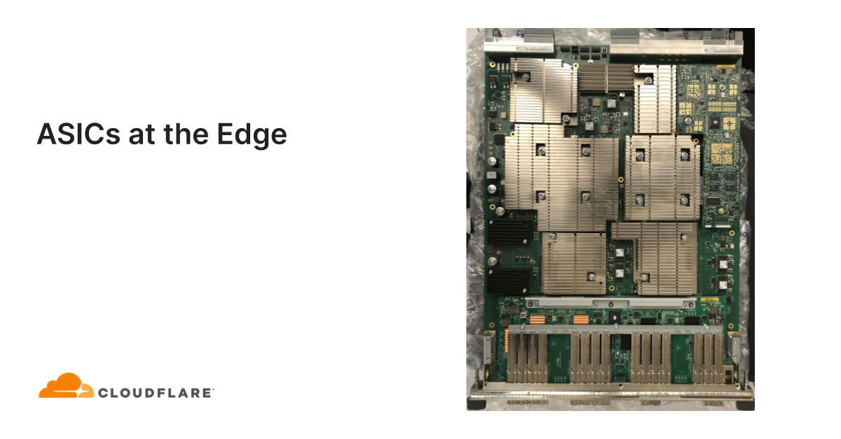
At Cloudflare we pride ourselves in our global network that spans more than 200 cities in over 100 countries. To handle all the traffic passing through our network, there are multiple technologies at play. So let’s have a look at one of the cornerstones that makes all of this work… ASICs. No, not the running shoes.

What’s an ASIC?

ASIC stands for Application Specific Integrated Circuit. The name already says it, it’s a chip with a very narrow use case, geared towards a single application. This is in stark contrast to a CPU (Central Processing Unit), or even a GPU (Graphics Processing Unit). A CPU is designed and built for general purpose computation, and does a lot of things reasonably well. A GPU is more geared towards graphics (it’s in the name), but in the last 15 years, there’s been a drastic shift towards GPGPU (General Purpose GPU), in which technologies such as CUDA or OpenCL allow you to use the highly parallel nature of the GPU to do general purpose computing. A good example of GPU use is video encoding, or more recently, computer vision, used in applications such as self-driving cars.

Unlike CPUs or GPUs, ASICs are built with a single function in mind. Great examples are the Google Tensor Processing Units (TPU), used to accelerate machine learning functions[1], or for orbital maneuvering[2], in which specific orbital maneuvers are encoded, like the Hohmann Transfer, used to move rockets (and their payloads) to a new orbit at a different altitude. And they are also heavily used in the networking industry. Technically, the use case in the network industry should be called an ASSP (Application Specific Standard Product), but network engineers are simple people, so we prefer to call it an ASIC.

Why an ASIC

ASICs have the major benefit of being hyper-efficient. The more complex hardware is, the more it will need cooling and power. As ASICs only contain the hardware components needed for their function, their overall size can be reduced, and so are their power requirements. This has a positive impact on the overall physical size of the network (devices don’t need to be as bulky to provide sufficient cooling), and helps reduce the power consumption of a data center.

Reducing hardware complexity also reduces the failure rate of the manufacturing process, and allows for easier production.

The downside is that you need to embed a lot of your features in hardware, and once a new technology or specification comes around, any chips made without that technology baked in, won’t be able to support it (VXLAN for example).

For network equipment, this works perfectly. Overall, the networking industry is slow-moving, and considerable time is taken before new technologies make it to the market (as can be seen with IPv6, MPLS implementations, xDSL availability, …). This means the chips don’t need to evolve on a yearly basis, and can instead be created on a much slower cycle, with bigger leaps in technology. For example, it took Broadcom two years to go from Tomahawk 3 to Tomahawk 4, but in that process they doubled the throughput. The benefits listed earlier are super helpful for network equipment, as they allow for considerable throughput in a small form factor.

Building an ASIC

As with chips of any kind, building an ASIC is a long-term process. Just like with CPUs, if there’s a defect in the hardware design, you have to start from scratch, and scrap the entire build line. As such, the development lifecycle is incredibly long. It starts with prototyping in an FPGA (Field Programmable Gate Array), in which chip designers can program their required functionality and confirm compatibility. All of this is done in a HDL (Hardware Description Language), such as Verilog.

Once the prototyping stage is over, they move to baking the new packet processing pipeline into the chip at a foundry. After that, no more changes can be made to the chip, as it’s literally baked into the hardware (unlike an FPGA, which can be reprogrammed). Further difficulty is added by the fact that there are a very small number of hardware companies that will buy ASICs in bulk to build equipment with; as such the unit cost can increase drastically.

All of this means that the iteration cycle of an ASIC tends to be on the slower side of things (compared to the yearly refreshes in the Intel Process-Architecture-Optimization model for example), and will usually be smaller incremental updates: For example, increases in port-speeds are incremental (1G → 10G → 25G → 40G → 100G → 400G → 800G → …), and are tied into upgrades to the SerDes (Serialiser/Deserialiser) part of the chip.

New protocol support is a lot harder, and might require multiple development cycles before it shows up in a chip.

What ASICs do

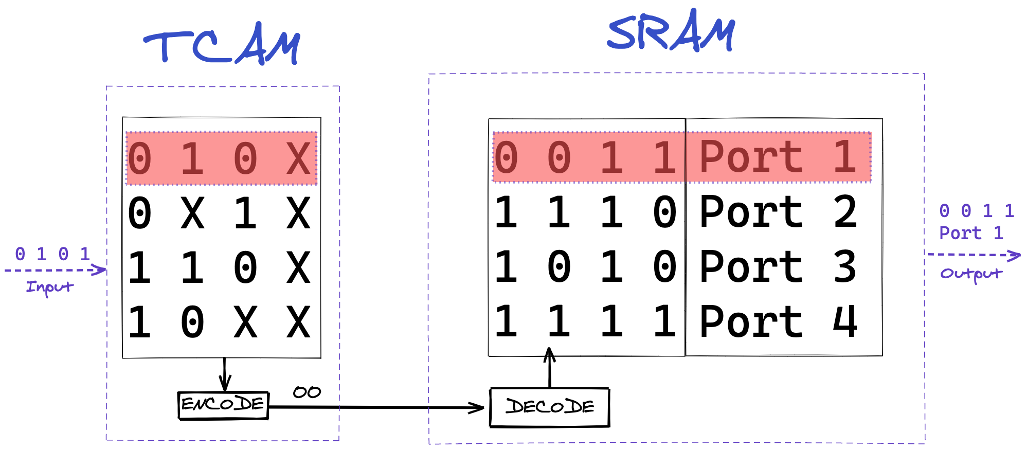
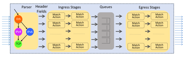
The ASICs in our network equipment are responsible for the switching and routing of packets, as well as being the first layer of defense (in the form of a stateless firewall). Due to the sheer nature of how fast packets get switched, fast memory access is a primary concern. Most ASICs will use a special sort of memory, called TCAM (Ternary Content-Addressable Memory). This memory will be used to store all sorts of lookup tables. These may be forwarding tables (where does this packet go), ACL (Access Control List) tables (is this packet allowed), or CoS (Class of Service) tables (which priority should be given to this packet)

CAM, and its more advanced sibling, TCAM, are fascinating kinds of memory, as they operate fundamentally different than traditional Random Access Memory (RAM). While you have to use a memory address to access data in RAM, with CAM and TCAM you can directly refer to the content you are looking for. It is a physical implementation of a key-value store.

In CAM you use the exact binary representation of a word, in a network application, that word is likely going to be an IP address, so 11001011.00000000.01110001.00000000 for example (203.0.113.0). While this is definitely useful, networks operate a big collection of IP addresses, and storing each individually would require significant memory. To remedy this memory requirement, TCAM can store three states, instead of the binary two. This third state, sometimes called ‘ignore’ state, allows for the storage of multiple sequential data words as a single entry.

In networking, these sequential data words are IP prefixes. So for the previous example, if we wanted to store the collection of that IP address, and the 254 IPs following it, in TCAM it would as follows: 11001011.00000000.01110001.XXXXXXXX (203.0.113.0/24). This storage method means we can ask questions of the ASIC such as “where should I send packets with the destination IP address of 203.0.113.19”, to which the ASIC can have a reply ready in a single clock cycle, as it does not need to run through all memory, but instead can directly reference the key. This reply will usually be a reference to a memory address in traditional RAM, where more data can be stored, such as output port, or firewall requirements for the packet.
ASICs at the Edge

To dig a bit deeper into what ASICs do in network equipment, let’s briefly go over some fundamentals.

Networking can be split into two primary components: routing and switching. Switching allows you to directly interconnect multiple devices, so they can talk with each other across the network. It’s what allows your phone to connect to your TV to play a new family video. Routing is the next level up. It’s the mechanism that interconnects all these switched networks into a network of networks, and eventually, the Internet.

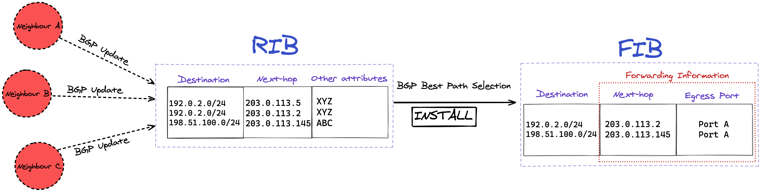
So routers are the devices responsible for steering traffic through this complex maze of networks, so it gets to its destination safely, and hopefully, as fast as possible. On the Internet, routers will usually use a routing protocol called BGP (Border Gateway Protocol) to exchange reachability information for a prefix (a collection of IP addresses), also called NLRI (Network Layer Reachability Information).

As with navigating the roads, there are multiple ways to get from point A to point B on the Internet. To make sure the router makes the right decision, it will store all of the reachability information in the RIB (Routing Information Base). That way, if anything changes with one route, the router still has other options immediately available.

With this information, a BGP daemon can calculate the ideal path to take for any given destination from its own point-of-view. This Cisco documentation explains the decision process the daemon goes through to calculate that ideal path.

Once we have this ideal path for a given destination, we should store this information, as it would be very inefficient to calculate this every single time we need to go there. The storage database is called the FIB (Forwarding Information Base). The FIB will be a subset of the RIB, as it will only ever contain the best path for a destination at any given time, while the RIB keeps all the available paths, even the non-ideal ones.

With these individual components, routers can make packets go from point A to point B in a blink of an eye.

Here’ are some of the more specific functions our ASICs need to perform:

  1. FIB install: Once the router has calculated its FIB, it’s important the router can access this as quickly as possible. To do so, the ASIC will install (write) this calculated FIB into the TCAM, so any lookups can happen as quickly as possible.
    ASICs at the Edge

  2. Packet forwarding lookups: as we need to know where to send a received packet, we look up this information in TCAM, which is, as we mentioned, incredibly fast.

  3. Stateless Firewall: while a router routes packets between destinations, you also want to ensure that certain packets don’t reach a destination at all. This can be done using either a stateless or stateful firewall. “State” in this case refers to TCP state, so the router would need to understand if a connection is new, or already established. As maintaining state is a complex issue, which requires storing tables, and can quickly consume a lot of memory, most routers will only operate a stateless firewall.
    Instead, stateful firewalls often have their own appliances. At Cloudflare, we’ve opted to move maintaining state to our compute nodes, as that severely reduces the state-table (one router for all state vs X metals for all state combined). A stateless firewall makes use of the TCAM again to store rules on what to do with specific types of packets. For example, one of the rules we employ at our edge is DENY-BOGON-RANGES , in which we discard traffic sourced from RFC1918 space (and other unroutable space). As this makes use of TCAM, it can all be done at line rate (the maximum speed of the interface).

  4. Advanced features, such as GRE encapsulation: modern networking isn’t just packet switching and packet routing anymore, and more advanced features are needed. One of these is encapsulation. With packet encapsulation, a system will put a data packet into another data packet. Using this technique, it’s possible to build a network on top of an existing network (an overlay). Overlays can be used to build a virtual backbone for example, in which multiple locations can be virtually connected through the Internet.
    While you can encapsulate packets on a CPU (we do this for Magic Transit), there are considerable challenges in doing so in software. As such, the ASIC can have built-in functionality to encapsulate a packet in a multitude of protocols, such as GRE. You may not want encapsulated packets to have to take a second trip through your entire pipeline, as this adds latency, so these shortcuts can also be built into the chip.

  5. MPLS, EVPN, VXLAN, SDWAN, SDN, …: I ran out of buzzwords to enumerate here, but while MPLS isn’t new (the first RFC was created in 2001), it’s a rather advanced requirement, just as the others listed, which means not all ASIC vendors will implement this for all their chips due to the increased complexity.

Vendor Landscape

At Cloudflare, we interact with both hardware and software vendors on a daily basis while operating our global network. As we’re talking about ASICs today, we’ll explore the hardware landscape, but some hardware vendors also have their own NOS (Network Operating System).
There’s a vast selection of hardware out there, all with different features and pricing. It can become incredibly hard to see the wood for the trees, so we’ll focus on 4 important distinguishing factors: Throughput (how many bits can the ASIC push through), buffer size (how many bits can the ASIC store in memory in case of resource contention), programmability (how easy is it for a third party programmer like Cloudflare to interact directly with the ASIC), feature set (how many advanced things outside of routing/switching can the ASIC do).

The landscape is so varied because different companies have different requirements. A company like Cloudflare has different expectations for its network hardware than your typical corner shop. Even within our own network we’ll have different requirements for the different layers that make up our network.

Broadcom

The elephant in the networking room (or is it the jumbo frame in the switch?) is Broadcom. Broadcom is a semiconductor company, with their primary revenue in the wired infrastructure segment (over 50% of revenue[3]). While they’ve been around since 1991, they’ve become an unstoppable force in the last 10 years, in part due to their reliance on Apple (25% of revenue). As a semiconductor manufacturer, their market dominance is primarily achieved by acquiring other companies. A great example is the acquisition of Dune Networks, which has become an excellent revenue generator as the StrataDNX series of ASIC (Arad, QumranMX, Jericho). As such, they have become the biggest ASIC vendor by far, and own 59% of the entire Ethernet Integrated Circuits market[4].

As such, they supply a lot of merchant silicon to Cisco, Juniper, Arista and others. Up until recently, if you wanted to use the Broadcom SDK to accelerate your packet forwarding, you have to sign so many NDAs you might get a hand cramp, which makes programming them a lot trickier. This changed recently when Broadcom open-sourced their SDK. Let’s have a quick look at some of their products.

Tomahawk

The Tomahawk line of ASICs are the bread-and-butter for the enterprise market. They’re cheap and incredibly fast. The first generation of Tomahawk chips did 3.2Tbps linerate, with low-latency switching. The latest generation of this chip (Tomahawk 4) does 25.6Tbps in a 7nm transistor footprint[5]). As you can’t have a cheap, fast, and full feature set for a single package, this means you lose out on features. In this case, you’re missing most of the more advanced networking technologies such as VXLAN, and you have no buffer to speak of.
As an example of a different vendor using this silicon, you can have a look at the Juniper QFX5200 switching platform.

StrataDNX (Arad, QumranMX, Jericho)

These chipsets came through the acquisition of Dune Networks, and are a collection of high-bandwidth, deep buffer (large amount of memory available to store (buffer) packets) chips, allowing them to be deployed in versatile environments, including the Cloudflare edge. The Arista DCS-7280SR that we run in some of our edge locations as edge routers run on the Jericho chipset. Since then, the chips have evolved, and with Jericho2, Broadcom now have a 10Tbps deep buffer chip[6]. With their fabric chip (this links multiple ASICs together), you can build switches with 48x400G ports[7] without much effort.
Cisco built their NCS5500 line of routers using the QumranMX[8].

Trident

This ASIC is an upgrade from the Tomahawk chipset, with a complex and extensive feature set, while maintaining high throughput rates. The latest Trident4 does 12.8Tbps at incredibly low latencies[9], making it an incredibly flexible platform. It unfortunately has no buffer space to speak of, which limits its scope for Cloudflare, as we need the buffer space to be able to switch between the different port speeds we have on our edge routers. The Arista 7050X and 7300X are built on top of this.

Intel

Intel is well known in the network industry for building stable and high-performance 10G NICs (Network Interface Controller). They’re not known for ASICs. They made an initial attempt with their acquisition of Fulcrum[10], which built the FM6000[11] series of ASIC, but nothing of note was really built with them. Intel decided to try again in 2019 with their acquisition of Barefoot. This small manufacturer is responsible for the Barefoot Tofino ASIC, which may well be a fundamental paradigm shift in the network industry.

Barefoot Tofino

The Tofino[12] is built using a PISA (Protocol Independent Switch Architecture), and using P4 (Programming Protocol-Independent Packet Processors)[13], you can program the data-plane (packet forwarding) as you see fit. It’s a drastic move away from the traditional method of networking, in which direct programming of the ASIC isn’t easily possible, and definitely not through a standard programming language. As an added benefit, P4 also allows you to perform a formal verification of your forwarding program, and be sure that it will do what you expect it to. Caveat: OpenFlow tried this, but unfortunately never really got much traction.
ASICs at the Edge[14]

There are multiple variations of the Tofino 1 available, but the top-end ASIC has a 6.5Tbps linerate capacity. As the ASIC is programmable, its featureset is as rich as you’d want it to be. Unfortunately, the chip does not come with a lot of buffer memory, so we can’t deploy these as edge devices (yet). Both Arista (7170 Series[15]) and Cisco (Nexus 34180YC and 3464C series[16]) have built equipment with the Tofino chip inside.

Mellanox

As some of you may know, Mellanox is the vendor that recently got acquired by Nvidia, which also provides our 25G NICs in our compute nodes. Besides NICs, Mellanox has a well-established line of ASICs, mostly for switching.

Spectrum

The latest iteration of this ASIC, Spectrum 3 offers 12.8Tbps switching capacity, with an extensive featureset, including Deep Packet Inspection and NAT. This chip allows for building dense high-speed port devices, going up to 25.6Tbps[17]. Buffering wise, there’s none to really speak of (64MB). Mellanox also builds their own hardware platforms. Unlike the other vendors below, they aren’t shipped with the Mellanox Operating System, instead, they offer you a variety of choices to run on top, including Cumulus Linux (which was also acquired by Nvidia 🤔).

As mentioned, while we use their NIC technology extensively, we currently don’t have any Mellanox ASIC silicon in our network.

Juniper

Juniper is a network hardware supplier, and currently the biggest supplier of network equipment for Cloudflare. As previously mentioned in the Broadcom section, Juniper buys some of their silicon from Broadcom, but they also have a significant lineup of home-grown silicon, which can be split into 2 families: Trio and Express.

Express

The Express family is the switching-skewed family, where bandwidth is a priority, while still maintaining a broad range of feature capabilities. These chips live in the same application landscape as the Broadcom StrataDNX chips.

Paradise (Q5)

The Q5 is the new generation of the Juniper switching ASIC[18]. While by itself it doesn’t boast high linerates (500Gbps), when combined into a chassis with a fabric chip (Clos network in this case), they can produce switches (or line cards) with up to 12Tbps of throughput capacity[19]. In addition to allowing for high-throughput, dense network appliances, the chip also comes with a staggering amount of buffer space (4GB per ASIC), provided by external HMC (Hybrid Memory Cube). In this HMC, they’ve also decided to put the FIB, MAC and other tables (so no TCAM).
The Q5 chip is used in their QFX1000 lineup of switches, which include the QFX10002-36Q, QFX10002-60C, QFX10002-72Q and QFX10008, all of which are deployed in our datacenters, as either edge routers or core aggregation switches.

ExpressPlus (ZX)

The ExpressPlus is the more feature-rich and faster evolution of the Paradise chip. It offers double the bandwidth per chip (1Tbps) and is built into a combined Clos-fabric reaching 6Tbps in a 2U form-factor (PTX10002). It also has an increased logical scale, which comes with bigger buffers, larger FIB storage, and more ACL space.

The ExpressPlus drives some of the PTX line of IP routers, together with its newest sibling, Triton.

Triton (BT)

Triton is the latest generation of ASIC in the Express family, with 3.6Tbps of capacity per chip, making way for some truly bandwidth-dense hardware. Both Triton and ExpressPlus are 400GE capable.

Trio

The Trio family of chips are primarily used in the feature-heavy MX routing platform, and is currently at its 5th generation.

ASICs at the Edge
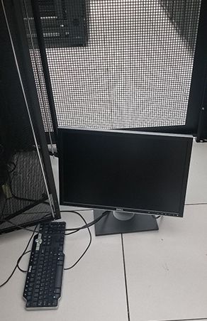
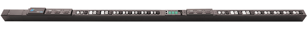
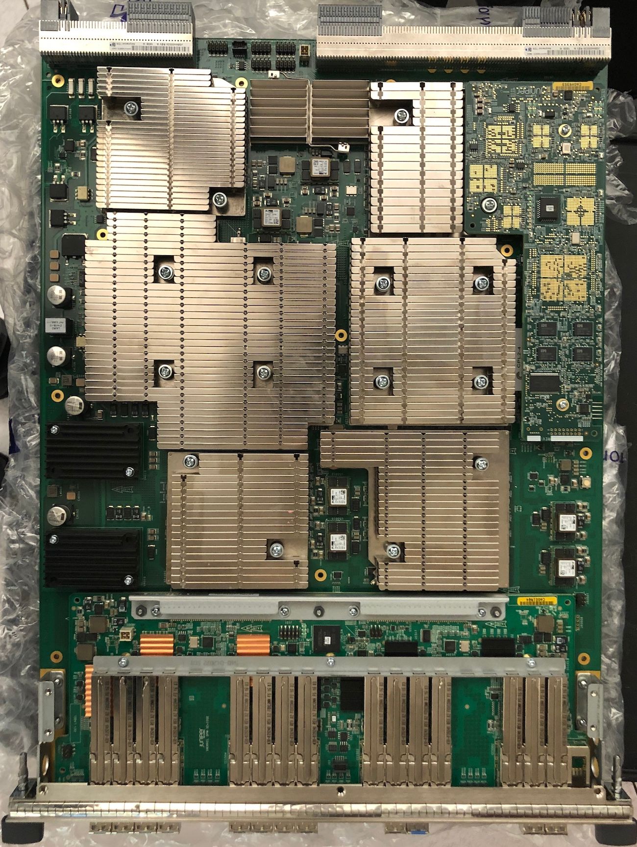
A Juniper MPC4E-3D-32XGE line card

Trio Eagle (Trio 4.0) (EA)

The Trio Eagle is the previous generation of the Trio Penta, and can be found on the MPC7E line cards for example. It’s a feature-rich ASIC, with a 400Gbps forwarding capacity, and significant buffer and TCAM capacity (as is to be expected from a routing platform ASIC)

Trio Penta (Trio 5.0) (ZT)

Penta is the new generation routing chip, which is built for the MX platform routers. On top of being a very beefy chip, capable of 500Gbps per ASIC, allowing Juniper to build line cards of up to 4Tbps of capacity, the chip also has a lot of baked in features, offering advanced hardware offloading for for example MACSec, or Layer 3 IPsec.

The Penta chip is packaged on the MPC10E and MPC11E line card, which can be installed in multiple variations of the MX chassis routers (MX480 included).

Cisco

Last but not least, there’s Cisco. As the saying goes “nobody ever got fired for buying Cisco”, they’re the biggest vendor of network solutions around. Just like Juniper, they have a mixed product fleet of merchant silicon, as well as home-grown. While we used to operate Cisco routers as edge routers (Cisco ASR 9000), this is no longer the case. We do still use them heavily for our ToR (Top-of-Rack) switching needs, utilizing both their Nexus 5000 series and Nexus 9000 series switches.

Bigsur

Bigsur is custom silicon developed for the Nexus 6000 line of switches (confusingly, the switches themselves are called Cisco Nexus 5672UP and Cisco Nexus 6001). In our specific model, the Cisco Nexus 5672UP, there’s 7 of them interconnected, providing 10G and 40G connectivity. Unfortunately Cisco is a lot more tight-lipped about their ASIC capabilities, so I can’t go as deep as I did with the Juniper chips. Feature-wise, there’s not a lot we require from them in our edge network. They’re simple Layer 2 forwarding switches, with no added requirements. Buffer wise, they use a system called Virtual Output Queueing, just like the Juniper Express chip. Unlike the Juniper silicon, the Bigsur ASIC doesn’t come with a lot of TCAM or buffer space.

Tahoe

The Tahoe is the Cisco ASIC found in the Cisco 9300-EX switches, also known as the LSE (Leaf Spine Engine). It offers higher-density port configurations compared to the Bigsur (1.6Tbps)[20]. Overall, this ASIC is a maturation of the Bigsur silicon, offering more advanced features such as advanced VXLAN+EVPN fabrics, greater port flexibility (10G, 25G, 40G and 100G), and increased buffer sizes (40MB). We use this ASIC extensively in both our edge data centers as well as in our core data centers.

Conclusion

A lot of different factors come into play when making the decision to purchase the next generation of Cloudflare network equipment. This post only scratches the surface of technical considerations to be made, and doesn’t come near any other factors, such as ecosystem contributions, openness, interoperability, or pricing. None of this would’ve been possible without the contributions from other network engineers—this post was written on the shoulders of giants. In particular, thanks to the excellent work by Jim Warner at UCSC, the engrossing book on the new MX platforms, written by David Roy (Day One: Inside the MX 5G), as well as the best book on the Juniper QFX lineup: Juniper QFX10000 Series by Douglas Richard Hanks Jr, and to finish it off, the Summary of Network ASICs post by Justin Pietsch.


  1. https://cloud.google.com/tpu/ ↩︎

  2. https://angel.co/company/spacex/jobs/744408-sr-fpga-asic-design-engineer ↩︎

  3. https://marketrealist.com/2017/02/wired-infrastructure-segment-protects-broadcom/ ↩︎

  4. https://www.wsj.com/articles/broadcom-lands-deals-to-place-components-in-apple-smartphones-11579821914 ↩︎

  5. https://www.globenewswire.com/news-release/2019/12/09/1958047/0/en/Broadcom-Ships-Tomahawk-4-Industry-s-Highest-Bandwidth-Ethernet-Switch-Chip-at-25-6-Terabits-per-Second.html ↩︎

  6. https://www.broadcom.com/products/ethernet-connectivity/switching/stratadnx/BCM88690 ↩︎

  7. https://www.ufispace.com/products/telco/core-edge/s9705-48d ↩︎

  8. https://www.ciscolive.com/c/dam/r/ciscolive/emea/docs/2019/pdf/BRKSPG-2900.pdf ↩︎

  9. https://www.broadcom.com/products/ethernet-connectivity/switching/strataxgs/bcm56880-series ↩︎

  10. https://newsroom.intel.com/news-releases/intel-to-acquire-fulcrum-microsystems/ ↩︎

  11. https://www.intel.com/content/dam/www/public/us/en/documents/datasheets/ethernet-switch-fm5000-fm6000-datasheet.pdf ↩︎

  12. https://barefootnetworks.com/products/brief-tofino/ ↩︎

  13. http://www.sigcomm.org/node/3503 ↩︎

  14. https://github.com/p4lang/p4lang.github.io/blob/master/assets/p4_switch_model-600px.png ↩︎

  15. https://www.arista.com/assets/data/pdf/Whitepapers/7170_White_Paper.pdf ↩︎

  16. https://www.barefootnetworks.com/press-releases/barefoot-networks-to-showcase-technologies-to-build-fast-and-resilient-networks-using-deep-insight-and-tofino-powered-cisco-nexus-switches-at-cisco-live-us-2019/ ↩︎

  17. https://www.mellanox.com/products/ethernet-switches/sn4000 ↩︎

  18. https://www.juniper.net/assets/us/en/local/pdf/whitepapers/2000599-en.pdf ↩︎

  19. https://www.juniper.net/assets/us/en/local/pdf/datasheets/1000531-en.pdf#page=7 ↩︎

  20. https://www.cisco.com/c/dam/global/fr_ch/solutions/data-center-virtualization/pdf/Cisco_Nexus_9300_EX_Platform.pdf#page=8 ↩︎

Getting to the Core: Benchmarking Cloudflare’s Latest Server Hardware

Post Syndicated from Brian Bassett original https://blog.cloudflare.com/getting-to-the-core/

Getting to the Core: Benchmarking Cloudflare’s Latest Server Hardware

Getting to the Core: Benchmarking Cloudflare’s Latest Server Hardware

Maintaining a server fleet the size of Cloudflare’s is an operational challenge, to say the least. Anything we can do to lower complexity and improve efficiency has effects for our SRE (Site Reliability Engineer) and Data Center teams that can be felt throughout a server’s 4+ year lifespan.

At the Cloudflare Core, we process logs to analyze attacks and compute analytics. In 2020, our Core servers were in need of a refresh, so we decided to redesign the hardware to be more in line with our Gen X edge servers. We designed two major server variants for the core. The first is Core Compute 2020, an AMD-based server for analytics and general-purpose compute paired with solid-state storage drives. The second is Core Storage 2020, an Intel-based server with twelve spinning disks to run database workloads.

Core Compute 2020

Earlier this year, we blogged about our 10th generation edge servers or Gen X and the improvements they delivered to our edge in both performance and security. The new Core Compute 2020 server leverages many of our learnings from the edge server. The Core Compute servers run a variety of workloads including Kubernetes, Kafka, and various smaller services.

Configuration Changes (Kubernetes)

Previous Generation Compute Core Compute 2020
CPU 2 x Intel Xeon Gold 6262 1 x AMD EPYC 7642
Total Core / Thread Count 48C / 96T 48C / 96T
Base / Turbo Frequency 1.9 / 3.6 GHz 2.3 / 3.3 GHz
Memory 8 x 32GB DDR4-2666 8 x 32GB DDR4-2933
Storage 6 x 480GB SATA SSD 2 x 3.84TB NVMe SSD
Network Mellanox CX4 Lx 2 x 25GbE Mellanox CX4 Lx 2 x 25GbE

Configuration Changes (Kafka)

Previous Generation (Kafka) Core Compute 2020
CPU 2 x Intel Xeon Silver 4116 1 x AMD EPYC 7642
Total Core / Thread Count 24C / 48T 48C / 96T
Base / Turbo Frequency 2.1 / 3.0 GHz 2.3 / 3.3 GHz
Memory 6 x 32GB DDR4-2400 8 x 32GB DDR4-2933
Storage 12 x 1.92TB SATA SSD 10 x 3.84TB NVMe SSD
Network Mellanox CX4 Lx 2 x 25GbE Mellanox CX4 Lx 2 x 25GbE

Both previous generation servers were Intel-based platforms, with the Kubernetes server based on Xeon 6262 processors, and the Kafka server based on Xeon 4116 processors. One goal with these refreshed versions was to converge the configurations in order to simplify spare parts and firmware management across the fleet.

As the above tables show, the configurations have been converged with the only difference being the number of NVMe drives installed depending on the workload running on the host. In both cases we moved from a dual-socket configuration to a single-socket configuration, and the number of cores and threads per server either increased or stayed the same. In all cases, the base frequency of those cores was significantly improved. We also moved from SATA SSDs to NVMe SSDs.

Core Compute 2020 Synthetic Benchmarking

The heaviest user of the SSDs was determined to be Kafka. The majority of the time Kafka is sequentially writing 2MB blocks to the disk. We created a simple FIO script with 75% sequential write and 25% sequential read, scaling the block size from a standard page table entry size of 4096KB to Kafka’s write size of 2MB. The results aligned with what we expected from an NVMe-based drive.

Getting to the Core: Benchmarking Cloudflare’s Latest Server Hardware

Core Compute 2020 Production Benchmarking

Cloudflare runs many of our Core Compute services in Kubernetes containers, some of which are multi-core. By transitioning to a single socket, problems associated with dual sockets were eliminated, and we are guaranteed to have all cores allocated for any given container on the same socket.

Another heavy workload that is constantly running on Compute hosts is the Cloudflare CSAM Scanning Tool. Our Systems Engineering team isolated a Compute 2020 compute host and the previous generation compute host, had them run just this workload, and measured the time to compare the fuzzy hashes for images to the NCMEC hash lists and verify that they are a “miss”.

Because the CSAM Scanning Tool is very compute intensive we specifically isolated it to take a look at its performance with the new hardware. We’ve spent a great deal of effort on software optimization and improved algorithms for this tool but investing in faster, better hardware is also important.

In these heatmaps, the X axis represents time, and the Y axis represents “buckets” of time taken to verify that it is not a match to one of the NCMEC hash lists. For a given time slice in the heatmap, the red point is the bucket with the most times measured, the yellow point the second most, and the green points the least. The red points on the Compute 2020 graph are all in the 5 to 8 millisecond bucket, while the red points on the previous Gen heatmap are all in the 8 to 13 millisecond bucket, which shows that on average, the Compute 2020 host is verifying hashes significantly faster.

Getting to the Core: Benchmarking Cloudflare’s Latest Server Hardware

Core Storage 2020

Another major workload we identified was ClickHouse, which performs analytics over large datasets. The last time we upgraded our servers running ClickHouse was back in 2018.

Configuration Changes

Previous Generation Core Storage 2020
CPU 2 x Intel Xeon E5-2630 v4 1 x Intel Xeon Gold 6210U
Total Core / Thread Count 20C / 40T 20C / 40T
Base / Turbo Frequency 2.2 / 3.1 GHz 2.5 / 3.9 GHz
Memory 8 x 32GB DDR4-2400 8 x 32GB DDR4-2933
Storage 12 x 10TB 7200 RPM 3.5” SATA 12 x 10TB 7200 RPM 3.5” SATA
Network Mellanox CX4 Lx 2 x 25GbE Mellanox CX4 Lx 2 x 25GbE

CPU Changes

For ClickHouse, we use a 1U chassis with 12 x 10TB 3.5” hard drives. At the time we were designing Core Storage 2020 our server vendor did not yet have an AMD version of this chassis, so we remained on Intel. However, we moved Core Storage 2020 to a single 20 core / 40 thread Xeon processor, rather than the previous generation’s dual-socket 10 core / 20 thread processors. By moving to the single-socket Xeon 6210U processor, we were able to keep the same core count, but gained 17% higher base frequency and 26% higher max turbo frequency. Meanwhile, the total CPU thermal design profile (TDP), which is an approximation of the maximum power the CPU can draw, went down from 165W to 150W.

On a dual-socket server, remote memory accesses, which are memory accesses by a process on socket 0 to memory attached to socket 1, incur a latency penalty, as seen in this table:

Previous Generation Core Storage 2020
Memory latency, socket 0 to socket 0 81.3 ns 86.9 ns
Memory latency, socket 0 to socket 1 142.6 ns N/A

An additional advantage of having a CPU with all 20 cores on the same socket is the elimination of these remote memory accesses, which take 76% longer than local memory accesses.

Memory Changes

The memory in the Core Storage 2020 host is rated for operation at 2933 MHz; however, in the 8 x 32GB configuration we need on these hosts, the Intel Xeon 6210U processor clocks them at 2666 MH. Compared to the previous generation, this gives us a 13% boost in memory speed. While we would get a slightly higher clock speed with a balanced, 6 DIMMs configuration, we determined that we are willing to sacrifice the slightly higher clock speed in order to have the additional RAM capacity provided by the 8 x 32GB configuration.

Storage Changes

Data capacity stayed the same, with 12 x 10TB SATA drives in RAID 0 configuration for best  throughput. Unlike the previous generation, the drives in the Core Storage 2020 host are helium filled. Helium produces less drag than air, resulting in potentially lower latency.

Core Storage 2020 Synthetic benchmarking

We performed synthetic four corners benchmarking: IOPS measurements of random reads and writes using 4k block size, and bandwidth measurements of sequential reads and writes using 128k block size. We used the fio tool to see what improvements we would get in a lab environment. The results show a 10% latency improvement and 11% IOPS improvement in random read performance. Random write testing shows 38% lower latency and 60% higher IOPS. Write throughput is improved by 23%, and read throughput is improved by a whopping 90%.

Previous Generation Core Storage 2020 % Improvement
4k Random Reads (IOPS) 3,384 3,758 11.0%
4k Random Read Mean Latency (ms, lower is better) 75.4 67.8 10.1% lower
4k Random Writes (IOPS) 4,009 6,397 59.6%
4k Random Write Mean Latency (ms, lower is better) 63.5 39.7 37.5% lower
128k Sequential Reads (MB/s) 1,155 2,195 90.0%
128k Sequential Writes (MB/s) 1,265 1,558 23.2%

CPU frequencies

The higher base and turbo frequencies of the Core Storage 2020 host’s Xeon 6210U processor allowed that processor to achieve higher average frequencies while running our production ClickHouse workload. A recent snapshot of two production hosts showed the Core Storage 2020 host being able to sustain an average of 31% higher CPU frequency while running ClickHouse.

Previous generation (average core frequency) Core Storage 2020 (average core frequency) % improvement
Mean Core Frequency 2441 MHz 3199 MHz 31%

Core Storage 2020 Production benchmarking

Our ClickHouse database hosts are continually performing merge operations to optimize the database data structures. Each individual merge operation takes just a few seconds on average, but since they’re constantly running, they can consume significant resources on the host. We sampled the average merge time every five minutes over seven days, and then sampled the data to find the average, minimum, and maximum merge times reported by a Compute 2020 host and by a previous generation host. Results are summarized below.

ClickHouse merge operation performance improvement
(time in seconds, lower is better)

Time Previous generation Core Storage 2020 % improvement
Mean time to merge 1.83 1.15 37% lower
Maximum merge time 3.51 2.35 33% lower
Minimum merge time 0.68 0.32 53% lower

Our lab-measured CPU frequency and storage performance improvements on Core Storage 2020 have translated into significantly reduced times to perform this database operation.

Conclusion

With our Core 2020 servers, we were able to realize significant performance improvements, both in synthetic benchmarking outside production and in the production workloads we tested. This will allow Cloudflare to run the same workloads on fewer servers, saving CapEx costs and data center rack space. The similarity of the configuration of the Kubernetes and Kafka hosts should help with fleet management and spare parts management. For our next redesign, we will try to further converge the designs on which we run the major Core workloads to further improve efficiency.

Special thanks to Will Buckner and Chris Snook for their help in the development of these servers, and to Tim Bart for validating CSAM Scanning Tool’s performance on Compute.

Anchoring Trust: A Hardware Secure Boot Story

Post Syndicated from Derek Chamorro original https://blog.cloudflare.com/anchoring-trust-a-hardware-secure-boot-story/

Anchoring Trust: A Hardware Secure Boot Story

Anchoring Trust: A Hardware Secure Boot Story

As a security company, we pride ourselves on finding innovative ways to protect our platform to, in turn, protect the data of our customers. Part of this approach is implementing progressive methods in protecting our hardware at scale. While we have blogged about how we address security threats from application to memory, the attacks on hardware, as well as firmware, have increased substantially. The data cataloged in the National Vulnerability Database (NVD) has shown the frequency of hardware and firmware-level vulnerabilities rising year after year.

Technologies like secure boot, common in desktops and laptops, have been ported over to the server industry as a method to combat firmware-level attacks and protect a device’s boot integrity. These technologies require that you create a trust ‘anchor’, an authoritative entity for which trust is assumed and not derived. A common trust anchor is the system Basic Input/Output System (BIOS) or the Unified Extensible Firmware Interface (UEFI) firmware.

While this ensures that the device boots only signed firmware and operating system bootloaders, does it protect the entire boot process? What protects the BIOS/UEFI firmware from attacks?

The Boot Process

Before we discuss how we secure our boot process, we will first go over how we boot our machines.

Anchoring Trust: A Hardware Secure Boot Story

The above image shows the following sequence of events:

  • After powering on the system (through a baseboard management controller (BMC) or physically pushing a button on the system), the system unconditionally executes the UEFI firmware residing on a flash chip on the motherboard.
  • UEFI performs some hardware and peripheral initialization and executes the Preboot Execution Environment (PXE) code, which is a small program that boots an image over the network and usually resides on a flash chip on the network card.
  • PXE sets up the network card, and downloads and executes a small program bootloader through an open source boot firmware called iPXE.
  • iPXE loads a script that automates a sequence of commands for the bootloader to know how to boot a specific operating system (sometimes several of them). In our case, it loads our Linux kernel, initrd (this contains device drivers which are not directly compiled into the kernel), and a standard Linux root filesystem. After loading these components, the bootloader executes and hands off the control to the kernel.
  • Finally, the Linux kernel loads any additional drivers it needs and starts applications and services.

UEFI Secure Boot

Our UEFI secure boot process is fairly straightforward, albeit customized for our environments. After loading the UEFI firmware from the bootloader, an initialization script defines the following variables:

Platform Key (PK): It serves as the cryptographic root of trust for secure boot, giving capabilities to manipulate and/or validate the other components of the secure boot framework.

Trusted Database (DB): Contains a signed (by platform key) list of hashes of all PCI option ROMs, as well as a public key, which is used to verify the signature of the bootloader and the kernel on boot.

These variables are respectively the master platform public key, which is used to sign all other resources, and an allow list database, containing other certificates, binary file hashes, etc. In default secure boot scenarios, Microsoft keys are used by default. At Cloudflare we use our own, which makes us the root of trust for UEFI:

Anchoring Trust: A Hardware Secure Boot Story

But, by setting our trust anchor in the UEFI firmware, what attack vectors still exist?

UEFI Attacks

As stated previously, firmware and hardware attacks are on the rise. It is clear from the figure below that firmware-related vulnerabilities have increased significantly over the last 10 years, especially since 2017, when the hacker community started attacking the firmware on different platforms:

Anchoring Trust: A Hardware Secure Boot Story

This upward trend, coupled with recent malware findings in UEFI, shows that trusting firmware is becoming increasingly problematic.

By tainting the UEFI firmware image, you poison the entire boot trust chain. The ability to trust firmware integrity is important beyond secure boot. For example, if you can’t trust the firmware not to be compromised, you can’t trust things like trusted platform module (TPM) measurements to be accurate, because the firmware is itself responsible for doing these measurements (e.g a TPM is not an on-path security mechanism, but instead it requires firmware to interact and cooperate with). Firmware may be crafted to extend measurements that are accepted by a remote attestor, but that don’t represent what’s being locally loaded. This could cause firmware to have a questionable measured boot and remote attestation procedure.

Anchoring Trust: A Hardware Secure Boot Story

If we can’t trust firmware, then hardware becomes our last line of defense.

Hardware Root of Trust

Early this year, we made a series of blog posts on why we chose AMD EPYC processors for our Gen X servers. With security in mind, we started turning on features that were available to us and set forth the plan of using AMD silicon as a Hardware Root of Trust (HRoT).

Platform Secure Boot (PSB) is AMD’s implementation of hardware-rooted boot integrity. Why is it better than UEFI firmware-based root of trust? Because it is intended to assert, by a root of trust anchored in the hardware, the integrity and authenticity of the System ROM image before it can execute. It does so by performing the following actions:

  • Authenticates the first block of BIOS/UEFI prior to releasing x86 CPUs from reset.
  • Authenticates the System Read-Only Memory (ROM) contents on each boot, not just during updates.
  • Moves the UEFI Secure Boot trust chain to immutable hardware.

This is accomplished by the AMD Platform Security Processor (PSP), an ARM Cortex-A5 microcontroller that is an immutable part of the system on chip (SoC). The PSB consists of two components:

On-chip Boot ROM

  • Embeds a SHA384 hash of an AMD root signing key
  • Verifies and then loads the off-chip PSP bootloader located in the boot flash

Off-chip Bootloader

  • Locates the PSP directory table that allows the PSP to find and load various images
  • Authenticates first block of BIOS/UEFI code
  • Releases CPUs after successful authentication
Anchoring Trust: A Hardware Secure Boot Story
  1. The PSP secures the On-chip Boot ROM code, loads the off-chip PSP firmware into PSP static random access memory (SRAM) after authenticating the firmware, and passes control to it.
  2. The Off-chip Bootloader (BL) loads and specifies applications in a specific order (whether or not the system goes into a debug state and then a secure EFI application binary interface to the BL)
  3. The system continues initialization through each bootloader stage.
  4. If each stage passes, then the UEFI image is loaded and the x86 cores are released.

Now that we know the booting steps, let’s build an image.

Build Process

Public Key Infrastructure

Before the image gets built, a public key infrastructure (PKI) is created to generate the key pairs involved for signing and validating signatures:

Anchoring Trust: A Hardware Secure Boot Story

Our original device manufacturer (ODM), as a trust extension, creates a key pair (public and private) that is used to sign the first segment of the BIOS (private key) and validates that segment on boot (public key).

On AMD’s side, they have a key pair that is used to sign (the AMD root signing private key) and certify the public key created by the ODM. This is validated by AMD’s root signing public key, which is stored as a hash value (RSASSA-PSS: SHA-384 with 4096-bit key is used as the hashing algorithm for both message and mask generation) in SPI-ROM.

Private keys (both AMD and ODM) are stored in hardware security modules.

Because of the way the PKI mechanisms are built, the system cannot be compromised if only one of the keys is leaked. This is an important piece of the trust hierarchy that is used for image signing.

Certificate Signing Request

Once the PKI infrastructure is established, a BIOS signing key pair is created, together with a certificate signing request (CSR). Creating the CSR uses known common name (CN) fields that many are familiar with:

  • countryName
  • stateOrProvinceName
  • localityName
  • organizationName

In addition to the fields above, the CSR will contain a serialNumber field, a 32-bit integer value represented in ASCII HEX format that encodes the following values:

  • PLATFORM_VENDOR_ID: An 8-bit integer value assigned by AMD for each ODM.
  • PLATFORM_MODEL_ID: A 4-bit integer value assigned to a platform by the ODM.
  • BIOS_KEY_REVISION_ID: is set by the ODM encoding a 4-bit key revision as unary counter value.
  • DISABLE_SECURE_DEBUG: Fuse bit that controls whether secure debug unlock feature is disabled permanently.
  • DISABLE_AMD_BIOS_KEY_USE: Fuse bit that controls if the BIOS, signed by an AMD key, (with vendor ID == 0) is permitted to boot on a CPU with non-zero Vendor ID.
  • DISABLE_BIOS_KEY_ANTI_ROLLBACK: Fuse bit that controls whether BIOS key anti-rollback feature is enabled.
Anchoring Trust: A Hardware Secure Boot Story

Remember these values, as we’ll show how we use them in a bit. Any of the DISABLE values are optional, but recommended based on your security posture/comfort level.

AMD, upon processing the CSR, provides the public part of the BIOS signing key signed and certified by the AMD signing root key as a RSA Public Key Token file (.stkn) format.

Putting It All Together

The following is a step-by-step illustration of how signed UEFI firmware is built:

Anchoring Trust: A Hardware Secure Boot Story
  1. The ODM submits their public key used for signing Cloudflare images to AMD.
  2. AMD signs this key using their RSA private key and passes it back to ODM.
  3. The AMD public key and the signed ODM public key are part of the final BIOS SPI image.
  4. The BIOS source code is compiled and various BIOS components (PEI Volume, Driver eXecution Environment (DXE) volume, NVRAM storage, etc.) are built as usual.
  5. The PSP directory and BIOS directory are built next. PSP directory and BIOS directory table points to the location of various firmware entities.
  6. The ODM builds the signed BIOS Root of Trust Measurement (RTM) signature based on the blob of BIOS PEI volume concatenated with BIOS Directory header, and generates the digital signature of this using the private portion of ODM signing key. The SPI location for signed BIOS RTM code is finally updated with this signature blob.
  7. Finally, the BIOS binaries, PSP directory, BIOS directory and various firmware binaries are combined to build the SPI BIOS image.

Enabling Platform Secure Boot

Platform Secure Boot is enabled at boot time with a PSB-ready firmware image. PSB is configured using a region of one-time programmable (OTP) fuses, specified for the customer. OTP fuses are on-chip non-volatile memory (NVM) that permits data to be written to memory only once. There is NO way to roll the fused CPU back to an unfused one.

Enabling PSB in the field will go through two steps: fusing and validating.

  • Fusing: Fuse the values assigned in the serialNumber field that was generated in the CSR
  • Validating: Validate the fused values and the status code registers

If validation is successful, the BIOS RTM signature is validated using the ODM BIOS signing key, PSB-specific registers (MP0_C2P_MSG_37 and MP0_C2P_MSG_38) are updated with the PSB status and fuse values, and the x86 cores are released

If validation fails, the registers above are updated with the PSB error status and fuse values, and the x86 cores stay in a locked state.

Let’s Boot!

With a signed image in hand, we are ready to enable PSB on a machine. We chose to deploy this on a few machines that had an updated, unsigned AMI UEFI firmware image, in this case version 2.16. We use a couple of different firmware update tools, so, after a quick script, we ran an update to change the firmware version from 2.16 to 2.18C (the signed image):

. $sudo ./UpdateAll.sh
Bin file name is ****.218C

BEGIN

+---------------------------------------------------------------------------+
|                 AMI Firmware Update Utility v5.11.03.1778                 |      
|                 Copyright (C)2018 American Megatrends Inc.                |                       
|                         All Rights Reserved.                              |
+---------------------------------------------------------------------------+
Reading flash ............... done
FFS checksums ......... ok
Check RomLayout ........ ok.
Erasing Boot Block .......... done
Updating Boot Block ......... done
Verifying Boot Block ........ done
Erasing Main Block .......... done
Updating Main Block ......... done
Verifying Main Block ........ done
Erasing NVRAM Block ......... done
Updating NVRAM Block ........ done
Verifying NVRAM Block ....... done
Erasing NCB Block ........... done
Updating NCB Block .......... done
Verifying NCB Block ......... done

Process completed.

After the update completed, we rebooted:

Anchoring Trust: A Hardware Secure Boot Story

After a successful install, we validated that the image was correct via the sysfs information provided in the dmidecode output:

Anchoring Trust: A Hardware Secure Boot Story

Testing

With a signed image installed, we wanted to test that it worked, meaning: what if an unauthorized user installed their own firmware image? We did this by downgrading the image back to an unsigned image, 2.16. In theory, the machine shouldn’t boot as the x86 cores should stay in a locked state. After downgrading, we rebooted and got the following:

Anchoring Trust: A Hardware Secure Boot Story

This isn’t a powered down machine, but the result of booting with an unsigned image.

Anchoring Trust: A Hardware Secure Boot Story

Flashing back to a signed image is done by running the same flashing utility through the BMC, so we weren’t bricked. Nonetheless, the results were successful.

Naming Convention

Our standard UEFI firmware images are alphanumeric, making it difficult to distinguish (by name) the difference between a signed and unsigned image (v2.16A vs v2.18C), for example. There isn’t a remote attestation capability (yet) to probe the PSB status registers or to store these values by means of a signature (e.g. TPM quote). As we transitioned to PSB, we wanted to make this easier to determine by adding a specific suffix: -sig  that we could query in userspace. This would allow us to query this information via Prometheus. Changing the file name alone wouldn’t do it, so we had to make the following changes to reflect a new naming convention for signed images:

  • Update filename
  • Update BIOS version for setup menu
  • Update post message
  • Update SMBIOS type 0 (BIOS version string identifier)

Signed images now have a -sig suffix:

~$ sudo dmidecode -t0
# dmidecode 3.2
Getting SMBIOS data from sysfs.
SMBIOS 3.3.0 present.
# SMBIOS implementations newer than version 3.2.0 are not
# fully supported by this version of dmidecode.

Handle 0x0000, DMI type 0, 26 bytes
BIOS Information
	Vendor: American Megatrends Inc.
	Version: V2.20-sig
	Release Date: 09/29/2020
	Address: 0xF0000
	Runtime Size: 64 kB
	ROM Size: 16 MB

Conclusion

Finding weaknesses in firmware is a challenge that many attackers have taken on. Attacks that physically manipulate the firmware used for performing hardware initialization during the booting process can invalidate many of the common secure boot features that are considered industry standard. By implementing a hardware root of trust that is used for code signing critical boot entities, your hardware becomes a ‘first line of defense’ in ensuring that your server hardware and software integrity can derive trust through cryptographic means.

What’s Next?

While this post discussed our current, AMD-based hardware platform, how will this affect our future hardware generations? One of the benefits of working with diverse vendors like AMD and Ampere (ARM) is that we can ensure they are baking in our desired platform security by default (which we’ll speak about in a future post), making our hardware security outlook that much brighter 😀.

Swiss-Swedish Diplomatic Row Over Crypto AG

Post Syndicated from Bruce Schneier original https://www.schneier.com/blog/archives/2020/10/swiss-swedish-diplomatic-row-over-crypto-ag.html

Previously I have written about the Swedish-owned Swiss-based cryptographic hardware company: Crypto AG. It was a CIA-owned Cold War operation for decades. Today it is called Crypto International, still based in Switzerland but owned by a Swedish company.

It’s back in the news:

Late last week, Swedish Foreign Minister Ann Linde said she had canceled a meeting with her Swiss counterpart Ignazio Cassis slated for this month after Switzerland placed an export ban on Crypto International, a Swiss-based and Swedish-owned cybersecurity company.

The ban was imposed while Swiss authorities examine long-running and explosive claims that a previous incarnation of Crypto International, Crypto AG, was little more than a front for U.S. intelligence-gathering during the Cold War.

Linde said the Swiss ban was stopping “goods” — which experts suggest could include cybersecurity upgrades or other IT support needed by Swedish state agencies — from reaching Sweden.

She told public broadcaster SVT that the meeting with Cassis was “not appropriate right now until we have fully understood the Swiss actions.”

EDITED TO ADD (10/13): Lots of information on Crypto AG.